Decoding Ball Grid Array (BGA) Technology: A Comprehensive Guide
Update Time: Dec 08, 2023 Readership: 1077
Contents
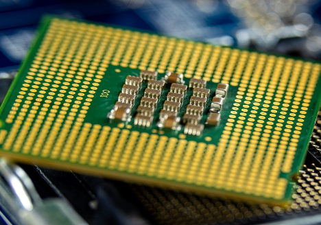
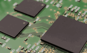
Ball Grid Array (BGA) packaging has emerged as a transformative technology in the realm of integrated circuits, revolutionizing the way electronic components are packaged and integrated into devices. Characterized by an array of solder balls on the chip's bottom surface, BGA has become a key enabler for miniaturization, increased integration, and superior performance in electronic devices. This article delves into the intricacies of BGA technology, exploring its advantages, applications, and so on.
What is A Ball Grid Array
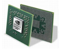
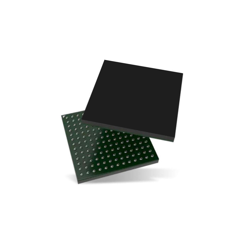
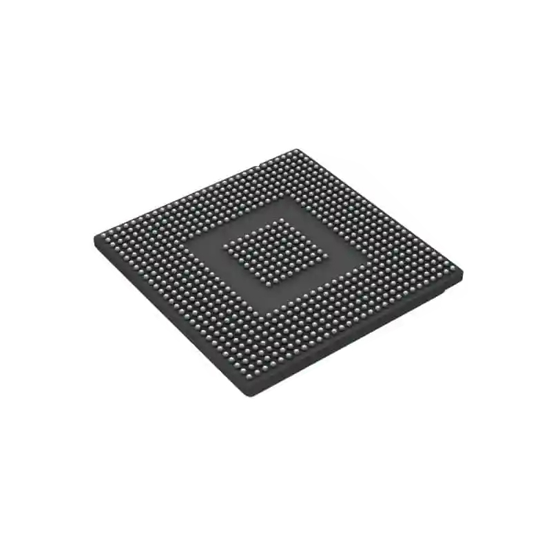
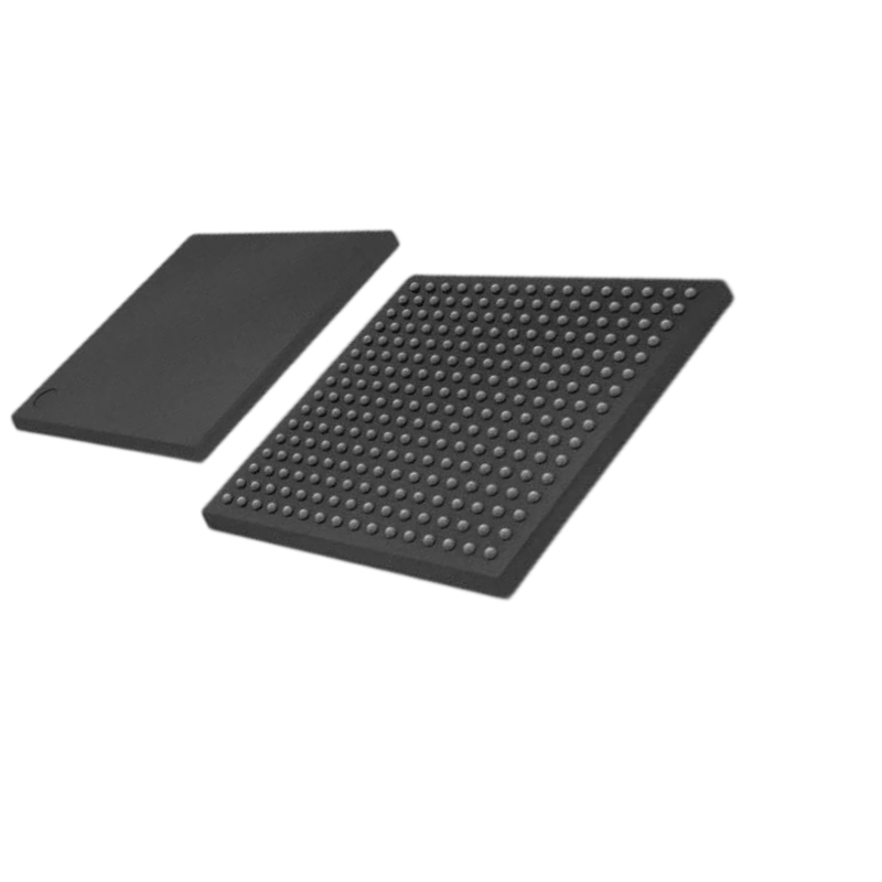
Ball Grid Array (BGA) packaging technology is a method used for the surface mounting of integrated circuits, commonly abbreviated as BGA. It involves a surface-adhesive packaging technique applied to integrated circuits, particularly microprocessors.
BGA, acronym for Ball Grid Array, is also known as "ball contact array package." It can be translated as "ball grid array," "network solder ball array," or "spherical array." BGA utilizes spherical contacts arranged in an array on the substrate's back, with the LSI assembled on the front (some BGA chips have terminals on the same side as the substrate). This packaging method is designed for surface mounting multi-pin LSIs.
BGA Package Types
-
CABGA (Chip Array Ball Grid Array): This BGA package type is characterized by the attachment of the integrated circuit to a substrate, and it can use either ceramic or plastic as the substrate material.
-
CBGA (Ceramic Ball Grid Array) and PBGA (Plastic Ball Grid Array): CBGA and PBGA both represent BGA packages where the integrated circuit is attached to a substrate made of either ceramic or plastic, respectively.
-
CTBGA (Thin Chip Array Ball Grid Array): CTBGA is a BGA package type with a thin chip array, contributing to a compact and space-efficient design.
-
CVBGA (Very Thin Chip Array Ball Grid Array): CVBGA takes thinness a step further, featuring a very thin chip array for applications requiring ultra-compact designs.
-
DSBGA (Die-Size Ball Grid Array): DSBGA is characterized by the fact that the package size closely matches the size of the integrated circuit die.
-
FBGA (Fine Ball Grid Array): FBGA features a fine pitch, indicating a tight arrangement of solder balls, contributing to a higher pin density.
-
FCmBGA (Flip Chip Molded Ball Grid Array): FCmBGA involves the flip-chip technology where the integrated circuit is flipped and mounted directly onto the substrate, enhancing thermal and electrical performance.
-
LBGA (Low-profile Ball Grid Array): LBGA is designed with a low-profile structure, suitable for applications where height constraints are crucial.
-
LFBGA (Low-profile Fine-pitch Ball Grid Array): LFBGA combines the characteristics of low-profile design with a fine pitch, offering a compact and high-performance solution.
-
MBGA (Micro Ball Grid Array): MBGA is characterized by its miniature size, making it suitable for applications demanding a small footprint.
-
MCM-PBGA (Multi-Chip Module Plastic Ball Grid Array): MCM-PBGA involves the integration of multiple chips within a single package, enhancing overall system integration.
-
PBGA (Plastic Ball Grid Array): PBGA features a plastic substrate and is widely used for its cost-effectiveness and versatility.
-
SuperBGA (SBGA): SuperBGA, or SBGA, represents an advanced form of BGA with enhanced features and capabilities.
-
TABGA (Tape Array BGA): TABGA involves a tape array, offering advantages in terms of manufacturing processes and design flexibility.
-
TBGA (Thin BGA): TBGA is characterized by its thin profile, suitable for applications where space is a critical factor.
-
TEPBGA (Thermally Enhanced Plastic Ball Grid Array): TEPBGA is designed to provide improved thermal performance, making it suitable for applications with high heat dissipation requirements.
-
TFBGA (Thin and Fine Ball Grid Array): TFBGA combines thinness with a fine pitch, offering a balance between compact design and high pin density.
-
UFBGA/UBGA (Ultra Fine Ball Grid Array): UFBGA or UBGA features an ultra-fine pitch, making it suitable for applications demanding extremely high pin density.
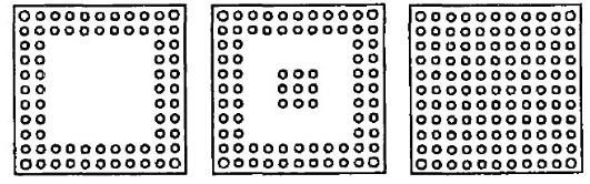
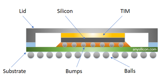
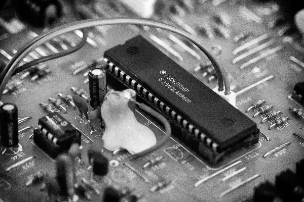
BGA Internal Construction
BGA packages utilize two primary methods to connect the silicon die to the substrate: Wirebond and FlipChip.
-
Wirebond BGA
In a wirebond BGA package, wires are employed to establish connections between the silicon die and the substrate. This method involves bonding thin wires from the die to specific points on the substrate, forming electrical connections.
-
FlipChip BGA
In a flipchip BGA package, bumps are used for connecting the silicon die to the substrate. The silicon die is flipped and attached directly to the substrate, with bumps serving as the connection points. This method provides advantages in terms of space efficiency and enhanced electrical performance.
Advantages of Ball Grid Array
Ball Grid Array (BGA) technology, a surface-adhesive packaging method for integrated circuits, offers several advantages, making it a preferred choice for various applications, particularly in permanently fixing devices like microprocessors.
-
High Density
BGA packaging addresses the challenge of packaging integrated circuits with hundreds of pins. Traditional packaging methods, such as Small-outline Integrated Circuit (SOIC) packages or Pinned Grid Array, face difficulties with smaller gaps between pins, making soldering complex. BGA overcomes this issue, allowing for a higher pin count without the risk of soldering challenges due to closer pin proximity during production.
-
Thermal Conductivity
BGA technology excels in thermal management compared to other packaging methods with separate pins. The BGA package exhibits lower thermal impedance between the package and the Printed Circuit Board (PCB). This efficient thermal conductivity facilitates the easy transfer of heat generated by the integrated circuit to the PCB, preventing chip overheating and ensuring optimal performance.
-
Low Inductance Pins
BGA packaging minimizes unnecessary inductance by employing shorter conductors. This reduction in inductance is crucial for high-speed electronic circuits, as it mitigates the risk of signal distortion. With the short distance between the BGA package and the PCB, coupled with low inductance pins, BGA technology offers superior electronic characteristics compared to pin devices.
-
Increased Pin Count
BGA packages can accommodate a higher number of pins compared to alternative packages like Dual In-line Package (DIP) or Quad Flat Package. This increased pin count enhances the overall functionality and capabilities of integrated circuits.
-
Short Average Wire Length
The bottom surface of the entire BGA device serves as pins, eliminating the need for peripheral placement. This design choice not only allows for more pins but also results in a shorter average wire length. The reduced wire length contributes to better high-speed performance, a crucial factor in modern electronic applications.
-
Precision in Soldering
The soldering of BGA packages requires precise control, typically achieved through factory equipment with automated procedures. This ensures accurate alignment and soldering of the numerous solder balls, addressing challenges associated with manual soldering processes.
-
No Socket Fixation
BGA package devices are not designed for socket fixation. Unlike some other packaging methods that allow easy removal and replacement of integrated circuits using sockets, BGAs are typically soldered directly onto the PCB.
Disadvantages of Ball Grid Array (BGA) Packaging
-
Non-Ductile Joint
Solder balls lack flexibility, making them prone to bending or breaking due to thermal and mechanical stress. Matching thermal characteristics between PCB and BGA helps but introduces challenges with RoHS-compatible solder.
-
RoHS-Compatible Solder Challenges
Use of lead-free solder may lead to issues like "head-in-pillow" and "pad cracks," reducing reliability in extreme environments. Solutions include underfilling and introducing a ductile coating.
-
Difficulty in Testing
Detecting defects post-soldering is challenging. Inspection methods include X-ray machines and circuit testing through IEEE 1149.1 JTAG. Visual X-ray inspection is expensive.
-
Difficulties in Circuit Development
During development, practical soldering is hard, leading to the use of sockets. Reliable sockets have limitations, and less reliable Zero Insertion Force (ZIF) sockets can be challenging, especially with small solder balls.
-
Equipment Cost
Reliable BGA soldering demands costly equipment. Hand-soldering is unreliable and limited to small devices. DIY methods with less sophisticated equipment have emerged due to the prevalence of lead-free and BGA ICs.
When Were Ball Grid Arrays Invented
The Ball Grid Array (BGA) packaging technology was first introduced in the 1990s. It was developed as an alternative to conventional Pin Grid Array (PGA) packaging, addressing challenges associated with PGA, where a large number of pins were densely positioned. BGA's design with a grid of solder balls on the bottom of the package offered advantages such as improved thermal performance, enhanced mechanical stability, and facilitated a more compact form factor. Since its introduction, BGA has become widely adopted in the electronics industry for mounting integrated circuits on printed circuit boards.
How to Solder Ball Grid Array
Column Grid Array vs Ball Grid Array
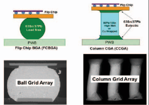
Column Grid Array (CGA) and Ball Grid Array (BGA) are both types of integrated circuit packaging technologies, each with its own set of characteristics.
Column Grid Array (CGA):
Design:
CGA utilizes columns (or pins) for electrical connections between the integrated circuit and the substrate.
Interconnection Method:
The electrical connections are made through the vertical columns, allowing for a different form of interconnection compared to the spherical contacts in BGA.
Mechanical Stability:
CGA is known for providing strong mechanical stability due to its column-based design.
Soldering Process:
Soldering the columns to the substrate requires precision, and the process may involve solder balls or other techniques.
Application:
CGA is used in certain applications where its specific characteristics, such as mechanical stability, are advantageous.
Ball Grid Array (BGA):
Design:
BGA utilizes a grid of spherical solder balls on the bottom of the package for electrical connections.
Interconnection Method:
The electrical connections are made through the spherical solder balls, providing a compact and efficient interconnection method.
Mechanical Stability:
BGA offers good mechanical stability, and its design minimizes the risk of damage during handling and assembly.
Soldering Process:
Soldering the spherical balls to the substrate is a common and well-established process, often achieved through reflow soldering.
Application:
BGA is widely used in various electronic devices, offering advantages such as high pin count, efficient use of space, and improved thermal characteristics.
Comparison:
Interconnection Style:
CGA uses vertical columns, while BGA uses a grid of spherical balls.
Mechanical Stability:
CGA is known for strong mechanical stability, but BGA also provides good stability with a more compact design.
Soldering Process:
CGA and BGA both involve soldering, but the specific techniques and challenges may vary.
Applications:
CGA may be chosen for applications where its specific attributes are crucial, while BGA is more versatile and widely used in various electronic devices.
What is the difference between BGA and LGA
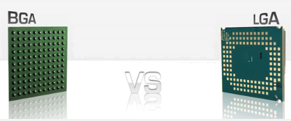
While both BGA and LGA are surface mount packaging technologies, BGA uses spherical solder balls for electrical connections, whereas LGA relies on flat surface pads. The main difference between Ball Grid Array (BGA) and Land Grid Array (LGA) lies in the style of interconnection and the physical structure of their contact points.
-
Ball Grid Array (BGA)
BGA features a grid of spherical solder balls on the bottom of the package.
The electrical connections are made through these spherical solder balls.
BGA is known for its compact design, high pin count, and efficient use of space.
It is commonly used in various electronic devices and is known for its good thermal characteristics.
-
Land Grid Array (LGA)
LGA, on the other hand, does not have solder balls as leads but a flat surface with pads.
The electrical connections are made through these flat pads on the surface of the package.
LGA is often used as a physical interface for microprocessors, where the contact can be made through an LGA socket or by soldering directly to the PCB.
LGA can provide good mechanical stability and is commonly used in applications where a solid contact surface is preferred.
What is the Difference Between PGA and BGA
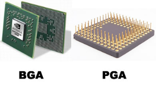
While PGAs use tiny pins arranged in a grid for electrical connections, BGAs use spherical solder balls for the same purpose. The transition from PGAs to BGAs has been driven by the advantages offered by BGA, such as better thermal characteristics, higher pin density, and improved reliability. The main difference between Pin Grid Array (PGA) and Ball Grid Array (BGA) lies in the style of interconnection and the physical structure of their contact points.
-
Pin Grid Array (PGA)
PGAs utilize tiny pins as leads for creating connections.
The electrical connections are made through these pins, which are arranged in a square grid featuring rows and columns.
PGA packages have been used historically and were prevalent before the widespread adoption of BGA.
The pins on a PGA package are typically longer and extend from the sides or the bottom of the package.
-
Ball Grid Array (BGA)
BGAs, on the other hand, utilize a grid of spherical solder balls on the bottom of the package for connections.
The electrical connections are made through these spherical solder balls.
BGA packages have gained popularity due to their compact design, high pin count, and efficient use of space.
The solder balls on a BGA package are typically shorter and are positioned on the entire bottom surface.
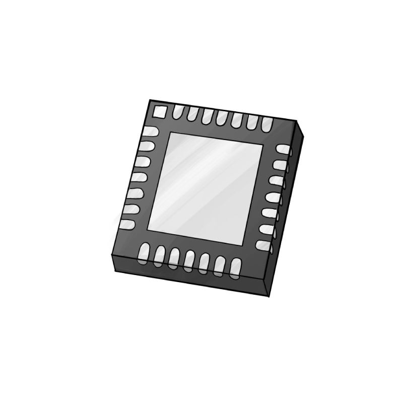
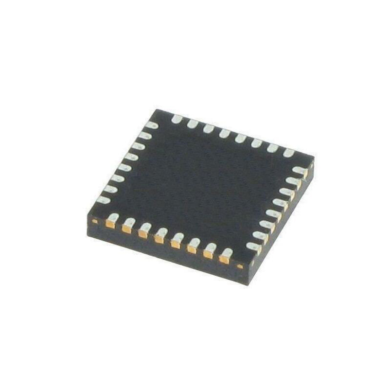
What is the Difference Between BGA and QFN
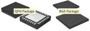
While both BGA and QFN are surface mount packages, their designs, electrical connections, and applications differ. BGA relies on a grid of solder balls for connections, making it suitable for various applications, while QFN has a flat bottom with exposed pads, making it more compact and ideal for space-constrained designs.
-
Package Design
BGA (Ball Grid Array): BGA packages have an array of solder balls on the bottom of the package, forming a grid. These solder balls provide electrical connections between the IC and the PCB.
QFN (Quad Flat No-Lead): QFN packages have a flat bottom with no protruding leads or pins. Instead, the electrical connections are made through exposed pads on the bottom surface.
-
Electrical Connections
BGA: The electrical connections in a BGA are established through solder balls, which are evenly distributed in a grid pattern on the package's underside.
QFN: QFN relies on exposed metal pads on the bottom surface of the package for soldering to the corresponding pads on the PCB.
-
Ease of Inspection and Rework
BGA: BGA packages can be more challenging to inspect and rework due to the hidden nature of solder balls beneath the package.
QFN: QFN packages are generally considered easier to inspect and rework because the soldering joints are visible and accessible.
-
Package Size and Applications
BGA: BGA packages are available in various sizes, and they are often used in applications where a high pin count is required, and space on the PCB is not a critical constraint.
QFN: QFN packages are known for their compact size and are often chosen for applications where space-saving is crucial. They are suitable for smaller and more space-constrained electronic devices.
-
Thermal Performance
BGA: BGA packages typically offer good thermal performance due to the large number of solder balls distributing heat evenly.
QFN: QFN packages also provide good thermal performance, as the exposed pads facilitate efficient heat dissipation.
What is the difference between BGA and micro BGA
BGA (Ball Grid Array) and micro BGA (μBGA) are both types of surface mount packaging used for integrated circuits (ICs) on printed circuit boards (PCBs). The primary difference between them lies in the ball pitch, which refers to the spacing between the solder balls on the bottom of the package.
-
BGA (Ball Grid Array)
BGA typically has larger ball-to-ball spacing, commonly around 1.0mm or 0.8mm.
This larger pitch allows for easier manufacturing and assembly processes, making it suitable for a wide range of applications.
BGA packages are larger compared to micro BGA.
-
Micro BGA (μBGA)
Micro BGA, as the name suggests, has a much smaller ball pitch, usually around 0.4mm or less.
The reduced pitch allows for a higher number of pins in a smaller package size.
Micro BGA is advantageous when space on the PCB is a critical factor, and designers need to fit more components in a limited area.
Due to the smaller size, micro BGA packages are more challenging to manufacture and require higher precision during assembly.
Final Words
Ball Grid Array (BGA) stands as a pivotal advancement in packaging technology, offering a myriad of benefits that have reshaped the landscape of integrated circuits. From facilitating the miniaturization of electronic devices to supporting higher levels of integration and providing a platform for improved performance, BGA has become synonymous with innovation in the semiconductor industry.
Read More:
7404 Integrated Circuit (IC): Datasheet, Pinout, Pin Diagram, Truth Table
7408 Integrated Circuit Datasheet: Pinout, Pin Diagram, Truth Table
Photonic Integrated Circuit: Definition, Disadvantage, Fabrication, Application
IC 74192 UP/Down Counter Datasheet PDF, Circuit, Pin Diagram
IC 74190 Datasheet, Working, Features, Application
CD4017BE CMOS Counter: Circuit, Pinout and Uses [Datasheet PDF]
IC 7490 Decade Counter Datasheet: Features, Pinout, Circuit and Working
What is Integrated Circuit Design?- How to Design?
Hybrid Integrated Circuits (Hybrid IC): Definition, Examples, Uses & Advantages
How Is a Microprocessor Different From an Integrated Circuit
Small Outline Integrated Circuit - SOIC
Popular Blogs
-
Small Outline Packag...
SOP (Small Outline Package) is a type of integra...
-
CD4440 IC: Datasheet...
The CD4440 IC is a stereo audio power amplifier ...
-
Advantages and Disad...
Operational amplifiers, or op-amps, offer a host...
-
Dual Inline Package ...
Dual in-line package, also known as DIP package ...
Hot Products
-
-
-
-
-
-
-
-
-
-
-
-
-
-
-
-
-
-
-
-
-
-
-
-
-
-
-
-
Infineon Technologies Corporation
100V Single N-Channel HEXFET Power MOSFET in a PQF...
-
Infineon Technologies Corporation
100V Single N-Channel HEXFET Power MOSFET in a D2-...
-
Infineon Technologies Corporation
150V Single N-Channel HEXFET Power MOSFET in a 5mm...
-
Infineon Technologies Corporation
150V Single N-Channel HEXFET Power MOSFET in a D2-...
-
Infineon Technologies Corporation
200V Single N-Channel HEXFET Power MOSFET in a D2-...
-
-
Infineon Technologies Corporation
250V Single N-Channel HEXFET Power MOSFET PDP Swit...
-
-
-
-
-
Infineon Technologies Corporation
60V Single N-Channel HEXFET Power MOSFET in a PQFN...
-
Infineon Technologies Corporation
A 30V Single N-Channel HEXFET Power MOSFET in a Di...
-
-
-
-
-
-
-
-
-
-
Popular Manufacturers