7408 Integrated Circuit Datasheet: Pinout, Pin Diagram, Truth Table
Update Time: Nov 15, 2023 Readership: 5926
Contents
The 7408 Integrated Circuit (IC) is a cornerstone in digital design, esteemed for its versatility and vital role in constructing basic logic gates. As a member of the 7400 series of transistor-transistor logic (TTL) chips, this IC is specifically designed as a quad 2-input AND gate. It consists of four independent gates, each capable of executing a logical AND function. This design allows each gate to output a high signal (logic level 1) exclusively when both its input signals are high. Conversely, if either or both inputs are low (logic level 0), the output remains low.
Beyond merely facilitating fundamental Boolean functions, the 7408 IC's structure enables the execution of more complex logic operations. Its adaptability renders it an ideal choice for rapidly developing digital systems that are both reliable and user-friendly. The IC's utility extends far beyond simple applications; its capacity to integrate seamlessly with other electronic components can lead to astounding results.
7408 Integrated Circuit Specification
|
7408 Integrated Circuit Specification |
Description |
|
Type |
Quad 2-Input AND Gate |
|
Number of Gates |
4 independent AND gates |
|
Number of Pins |
14 |
|
Supply Voltage (Vcc) |
Typically 4.75V to 5.25V (TTL level) |
|
Input Voltage (High) |
Minimum 2V (for a high-level input) |
|
Input Voltage (Low) |
Maximum 0.8V (for a low-level input) |
|
Output Voltage (High) |
Close to Vcc (when output is high) |
|
Output Voltage (Low) |
Close to 0V (when output is low) |
|
Operating Temperature |
Usually 0°C to 70°C |
|
Fan-out |
10 TTL loads |
|
Propagation Delay |
Approximately 10-15 ns |
|
Power Dissipation |
About 10-20 mW per gate |
|
Package Type |
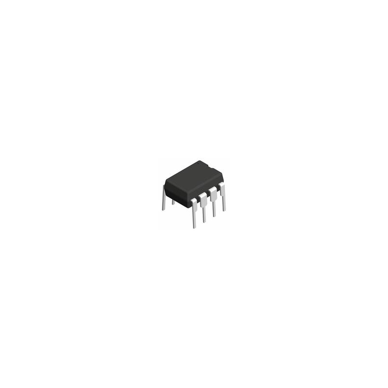
Dual In-line Package (DIP) |
7408 IC Name
IC 7408, more formally known as the Quad 2-Input AND Gate Integrated Circuit, is a fundamental component in the realm of digital electronics. This chip is part of the larger 7400 series of transistor-transistor logic (TTL) circuits, which are widely used for their reliability and ease of integration.
7408 Quad 2-input AND Gate Manufacturer
The 7408 is a commonly used integrated circuit (IC) that belongs to the 74xx series of ICs. The 74xx series is a family of digital logic ICs, and each IC within this series performs a specific logic function. The 7408, in particular, is a quad 2-input AND gate. It has four AND gates, each with two inputs.
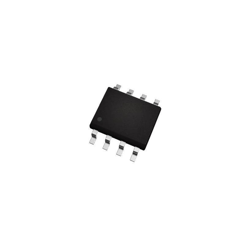
As for the manufacturer of the 7408 IC, multiple semiconductor companies have produced and continue to manufacture ICs within the 74xx series.
Texas Instruments (TI): Texas Instruments is a major semiconductor manufacturer that produces a wide range of ICs, including those in the 74xx series.
Fairchild Semiconductor: Fairchild Semiconductor, now part of ON Semiconductor, has a history of producing ICs, and they were one of the early manufacturers of 74xx series logic ICs.
NXP Semiconductors: NXP, a semiconductor company that originated from Philips Semiconductors, is another manufacturer known for producing logic ICs.
STMicroelectronics: STMicroelectronics is a global semiconductor company that manufactures a variety of ICs, including those in the 74xx series.
When working with or sourcing the 7408 IC, you may find versions from different manufacturers, but they are generally interchangeable as long as they adhere to the standard specifications of the 74xx series.
7408 Integrated Circuit Features
Four 2-Input Logic AND Gates: The IC contains four independent AND gates, each with two inputs. This configuration allows for multiple logical operations within a single chip, making it ideal for complex digital circuits.
Compatibility with Various Logic Families: The outputs of the 7408 IC can directly interface with several logic families, including CMOS (Complementary Metal-Oxide-Semiconductor), NMOS (N-Channel MOSFET), and TTL (Transistor-Transistor Logic). This interoperability is crucial for its integration into a wide range of digital systems.
Large Operating Voltage Range: The IC functions effectively over a broad range of voltage levels, typically between 4.75V and 5.25V for standard TTL versions. This makes it suitable for various power environments and ensures reliable operation under fluctuating power conditions.
Wide Operating Conditions: It is designed to operate under a broad spectrum of environmental conditions, which is essential for applications in different climates and settings. The typical operating temperature ranges from 0°C to 70°C, catering to a wide array of operational requirements.
Legacy Status and Recommendation for New Designs: While the 7408 has been a staple in digital circuit design, it is not recommended for new designs due to advancements in technology and the availability of better alternatives. For newer applications, especially where power efficiency and speed are concerns, the 74LS08 is recommended. The 74LS08 is a low-power Schottky version, which offers advantages like lower power consumption and faster switching times compared to the standard TTL 7408.
Fan-out Capability: The IC 7408 can drive multiple inputs in subsequent stages, known as fan-out. This feature is essential for cascading multiple gates or circuits without the need for additional amplification.
7408 IC Pinout
The 7408 IC, a Quad 2-Input AND Gate, has a standard pinout configuration typical of many integrated circuits, especially those in the 7400 series.
Pin 1 - A Input Gate 1: This is the first input for the first AND gate.
Pin 2 - B Input Gate 1: This is the second input for the first AND gate.
Pin 3 - Y Output Gate 1: This is the output for the first AND gate.
Pin 4 - A Input Gate 2: This is the first input for the second AND gate.
Pin 5 - B Input Gate 2: This is the second input for the second AND gate.
Pin 6 - Y Output Gate 2: This is the output for the second AND gate.
Pin 7 - Ground: This pin is connected to the ground or the negative side of the power supply.
Pin 8 - Y Output Gate 3: This is the output for the third AND gate.
Pin 9 - B Input Gate 3: This is the second input for the third AND gate.
Pin 10 - A Input Gate 3: This is the first input for the third AND gate.
Pin 11 - Y Output Gate 4: This is the output for the fourth AND gate.
Pin 12 - B Input Gate 4: This is the second input for the fourth AND gate.
Pin 13 - A Input Gate 4: This is the first input for the fourth AND gate.
Pin 14 - Vcc - Positive Supply: This pin is connected to the positive side of the power supply.
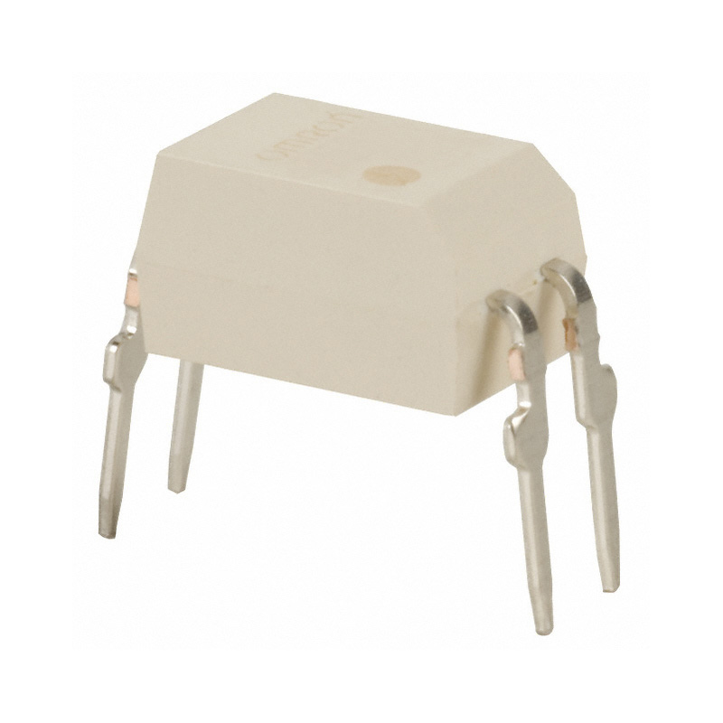
This 14-pin configuration allows the 7408 IC to house four independent AND gates, making it a compact and efficient component for performing logical operations in various digital circuits. The dual in-line package (DIP) of the IC is designed for easy insertion into breadboards or soldering onto printed circuit boards (PCBs). The clear separation of each gate's input and output pins on the IC makes it convenient for circuit designers to utilize the 7408 in complex designs without interference between gates.
7408 IC Pin Diagram
7408 IC Truth Table
The 7408 IC, which consists of four 2-input AND gates, has a straightforward truth table that reflects the basic logic of an AND gate.
|
A (Input) |
B (Input) |
Y (Output) |
|
0 |
0 |
0 |
|
0 |
1 |
0 |
|
1 |
0 |
0 |
|
1 |
1 |
1 |
In this table:
"A" and "B" represent the two inputs for each AND gate.
"Y" represents the output.
"0" and "1" represent the low (0V) and high (usually 5V in TTL logic) logic levels, respectively.
The output (Y) of an AND gate is high (1) only when both inputs (A and B) are high (1). In all other cases—where either or both inputs are low (0)—the output is low (0). This logic is the same for all four AND gates in the 7408 IC.
7408 Integrated Circuit Applications
Basic Logic Circuits: As a basic AND gate, the 7408 is used in constructing elementary logic functions and operations.
Digital Systems: It's integral in building more complex digital systems like computers, microprocessors, and microcontrollers where logical decision making is required.
Arithmetic Circuits: The 7408 is used in designing arithmetic circuits such as half adders and full adders, which are fundamental in computing operations.
Control Systems: It's used in control circuits for machines and processes, where specific conditions must be met before an action is triggered.
Input/Output Interface: The 7408 can be used to interface inputs and outputs in a system, ensuring that a certain combination of input signals is present before an output is activated.
Signal Gating: In signal processing, the 7408 can be used for gating signals, allowing a signal to pass through only when certain conditions are met.
Alarm Systems: It’s used in alarm systems, where multiple conditions (like sensor inputs) must be satisfied to trigger an alarm.
Data Processing: In data processing systems, it is used for implementing logical operations on data.
Educational and Experimental Projects: Due to its simplicity, the 7408 is widely used in educational setups to teach logic gate functions and in experimental projects for testing logic circuits.
Timing Circuits: It can also be used in timing circuits where the output depends on the combination of multiple input signals.
7408 IC Equivalent
Each of these ICs serves as a functional equivalent to the 7408, but they offer different advantages in terms of power consumption, switching speeds, and voltage range compatibility, making them suitable for various applications.
|
7408 Integrated Circuit Equivalent |
Description |
|
SN7408 |
Similar to 7408, part of Texas Instruments SN series |
|
74LS08 |
Low-power Schottky version, faster switching times, lower power consumption |
|
74HC08 |
High-speed CMOS version, operates at higher speeds, wider voltage range compatibility |
|
74HCT08 |
High-Speed CMOS with TTL compatible inputs |
|
CD4081 |
CMOS version, broader voltage range (3V to 18V) |
|
MC14008 |
CMOS version like CD4081, suitable for higher voltage range applications |
7408 Integrated Circuit Absolute Maximum Ratings
These absolute maximum ratings are critical to the proper use and longevity of the IC 7408. Exceeding these limits can result in damage to the IC or degradation of its performance. Always ensure that the operating conditions fall within these specified ranges to maintain the IC's integrity and functionality.
-
Maximum Propagation Delay: The IC 7408 features a maximum propagation delay of 10 nanoseconds (ns). This rating indicates the maximum time it takes for a change in input to be reflected at the output, which is crucial for timing and synchronizing in high-speed digital circuits.
-
Operating Temperature Range: The IC can operate effectively within a temperature range of -55°C to 125°C. This wide temperature range ensures reliable performance in various environmental conditions, from extreme cold to high-temperature scenarios, making the IC suitable for industrial and military applications.
-
Storage Temperature Range: The storage temperature range of -65°C to +150°C allows the IC to be stored safely under extreme conditions without affecting its functionality. This broad range is important for ensuring the long-term integrity of the IC when not in use.
-
High-Speed Operation: The IC is capable of operating at high speeds, up to 10 MHz. This characteristic makes it suitable for high-speed digital applications where rapid processing and response times are essential.
7408 Integrated Circuit Dimension
14-Pin DIP
Read More:
7404 Integrated Circuit (IC): Datasheet, Pinout, Pin Diagram, Truth Table
Photonic Integrated Circuit: Definition, Disadvantage, Fabrication, Application
What is Integrated Circuit Design?- How to Design?
Hybrid Integrated Circuits (Hybrid IC): Definition, Examples, Uses & Advantages
How Is a Microprocessor Different From an Integrated Circuit
Small Outline Integrated Circuit - SOIC
Different Types of IC [Integrated Circuit]
IC 74192 UP/Down Counter Datasheet PDF, Circuit, Pin Diagram
IC 74190 Datasheet, Working, Features, Application
CD4017BE CMOS Counter: Circuit, Pinout and Uses [Datasheet PDF]
IC 7490 Decade Counter Datasheet: Features, Pinout, Circuit and Working
Extended Reading
 FAQ
FAQ
-
How many gates will be there in a IC 7404 chip?
The IC 7404 is a hex inverter chip, and it indeed contains six NOT gates. Each NOT gate has a single input and produces the inverted output of that input. The 7404 is part of the 74xx series of integrated circuits, which consists of various digital logic gates and other components. The number 7404 specifically indicates a hex inverter, and the number 6 signifies the total count of inverters on the chip.
-
What does 74 mean in IC?
The 74 in an Integrated Circuit (IC) number, like in the 7408, indeed signifies that the IC belongs to the TTL (Transistor-Transistor Logic) series designed for commercial temperature grades. This series is engineered to operate effectively in a temperature range that is typical for commercial applications, typically up to 70°C. Originally, there were two main grades for these ICs: the military grade with the prefix 54 and the commercial grade with the prefix 74. The military-grade ICs were designed to withstand more extreme conditions, including a higher temperature range (up to 125°C). The commercial grade, or the 74 series, were developed later as a more cost-effective solution for non-military applications, where such extreme temperature resilience was not necessary.
-
What is the 1st pin on a 7408?
In a 7408 Integrated Circuit, which comprises four AND gates, Pin 1 is designated as the first input (A1) for the first AND gate.
-
How many gates are there in a regular 7408 chip?
A regular 7408 chip actually contains four AND logic gates, not three. Each of these gates operates independently and can produce an output based on the combination of its two input signals. In digital electronics, an AND gate is a basic logic gate that outputs a high signal (1) only when both of its inputs are high (1).
-
What is the function of 7408?
The 7408 IC is designed to build basic logic gates.
Popular Blogs
-
PCA9617ADPJ Datashee...
The PCA9617ADPJ is a signal buffer and repeater ...
-

D882 Transistor Pino...
The D882 transistor is a commonly used NPN bipol...
-
C1815 Transistor Dat...
The C1815 is a general purpose NPN transistor us...
-
C945 Transistor Data...
The C945 transistor is a small, low-power NPN bi...


