Infineon TDA21472 Datasheet: OptiMOS™ Powerstage DC-DC Converter Voltage Regulator
Update Time: Mar 01, 2024 Readership: 362
Contents

The TDA21472 OptiMOS™ Powerstage is a cutting-edge DC-DC converter voltage regulator designed to meet the demanding requirements of modern electronics. With a range of innovative features, this power stage is poised to revolutionize power delivery in various applications, from CPUs to GPUs and DDR memory arrays.
TDA21472 Features
Co-Packaged Design
The TDA21472 integrates a driver, Schottky diode, and high-side and low-side MOSFETs into a single package, optimizing space and simplifying implementation.
Enhanced Current Sensing
With a 5-mV/A on-chip MOSFET current sensing mechanism, coupled with temperature-compensated reporting, the TDA21472 achieves superior accuracy in current sensing, crucial for reliable system performance.
Wide Voltage Range
Operating with an input voltage (VIN) range of 4.25 V to 16 V, and VCC and VDRV supply ranging from 4.25 V to 5.5 V, the TDA21472 offers versatility in various power supply configurations.
High Output Capability
Capable of delivering an output current of up to 70 A, this power stage ensures robust performance even under heavy loads.
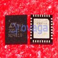
TDA21472 Pinout
The TDA21472 is a synchronous buck converter integrated circuit (IC) manufactured by Infineon Technologies. It integrates a low quiescent-current synchronous buck gate-driver IC, along with a Schottky diode, and high-side and low-side MOSFETs, in a single package.
Power Ground (PGND): Pins 5, 7-9, 20-24, 40. These pins connect to the power ground and also serve as the ground connection for the low-side MOSFET.
Signal Ground (LGND): Pin 2. This pin is the signal ground, and all other signal pins are referenced to this ground.
Input Voltage (VIN): Pin 1. This pin supplies the input voltage to the IC.
Bootstrap Capacitor (BOOT): Pin 32. This pin connects to the bootstrap capacitor, which provides the gate drive voltage for the high-side MOSFET.
Enable (EN): Pin 3. This pin controls the enable/disable functionality of the IC. A logic high enables the IC, while a logic low disables it.
Switching Node (SW): Pin 10-19. This pin is the high current switching node of the synchronous buck converter.
Low-Side MOSFET Driver (GATEL): Pin 6, 41. This pin is the low-side MOSFET driver output. It can be connected to a test point to observe the waveform.
Other Pins: Several other pins are present on the IC for functions like soft-start, feedback voltage, and fault protection.
TDA21472 Advanced Functionality
High-Speed Operation
Operating at frequencies of up to 1.5 MHz, the TDA21472 enables high-performance transient response, reducing the need for large output inductance and capacitance while maintaining exceptional efficiency.
Comprehensive Protection
Equipped with features such as VCC/VDRV under-voltage lockout (UVLO), thermal shutdown, and cycle-by-cycle over-current protection, the TDA21472 ensures the safety and longevity of the system.
Power Saving Modes
The power stage includes a deep-sleep mode, significantly reducing power consumption during idle periods, ideal for systems operating in low-power states.
TDA21472 Application Flexibility
Tailored for Server Applications
Optimized for CPU core power delivery in server applications, the TDA21472 meets the stringent requirements of the server market, making it equally suitable for GPU and DDR memory designs.
Body-Braking Support
Supporting Body-Braking load transient, the TDA21472 enhances transient performance by quickly disabling MOSFETs in response to PWM tri-state signals.
Diode Emulation Mode
Through PWM tri-state signals, the power stage supports diode emulation mode, enhancing light-load efficiency by preventing conduction loss caused by negative inductor current.
TDA21472 Block Diagram
TDA21472 Product Validation and Reliability
Industrial Qualification
The TDA21472 is qualified for industrial applications according to the relevant tests of JEDEC47/20/22, ensuring reliability and durability in harsh operating environments.
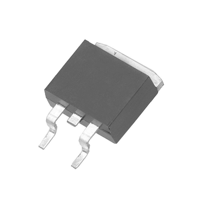
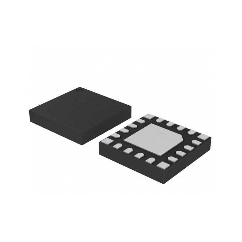
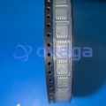
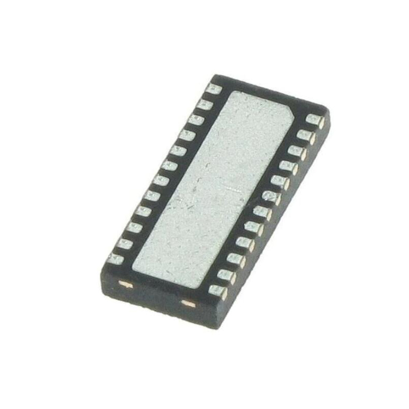
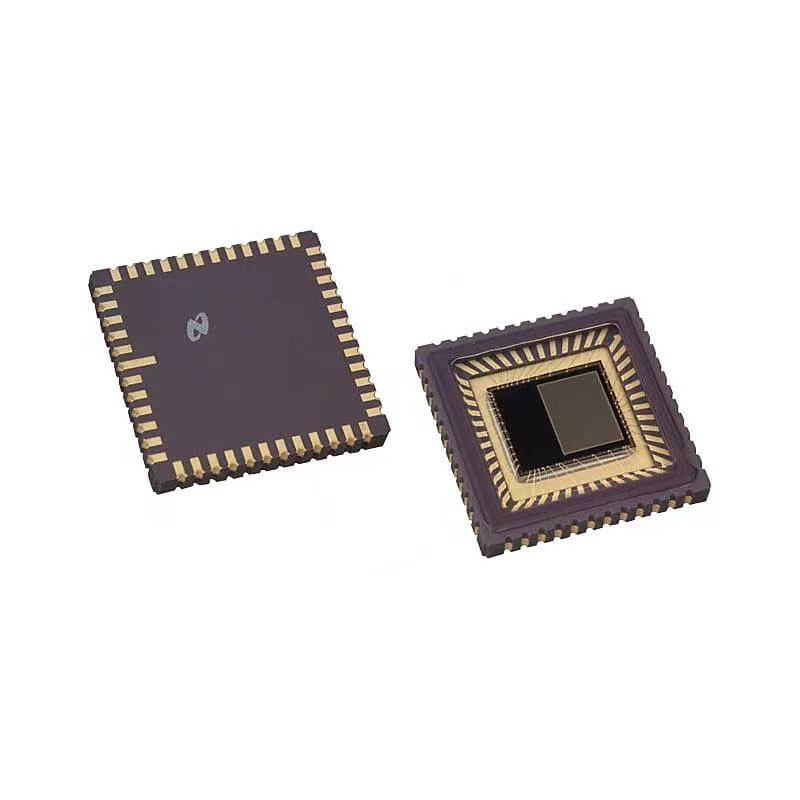
TDA21472 Package
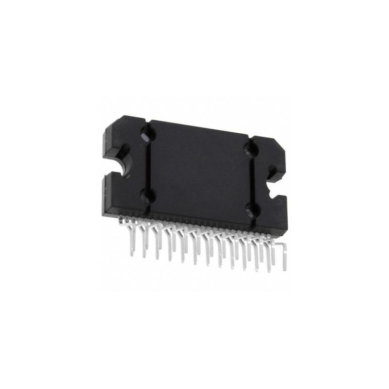
The TDA21472, a formidable DC-DC converter voltage regulator, is encapsulated within a PQFN (Plastic Quad Flat No-Lead) package measuring 5 mm x 6 mm. This compact yet robust packaging is engineered to optimize space utilization while ensuring efficient heat dissipation and reliable electrical connections.
The PQFN package dimensions of 5 mm x 6 mm strike an optimal balance between compactness and ease of implementation. Its flat, no-lead design simplifies surface mount assembly processes, enhancing manufacturability and reducing production costs.
Conclusion
The TDA21472 OptiMOS™ Powerstage represents a paradigm shift in DC-DC converter voltage regulation. With its integrated design, advanced features, and unparalleled performance, it offers a versatile solution for a wide range of applications, from high-performance computing to industrial systems. Whether it's maximizing efficiency, ensuring system reliability, or reducing footprint, the TDA21472 sets a new standard in power delivery technology.
TDA21472 In Stock: 5411 Pcs
Popular Blogs
-
Small Outline Packag...
SOP (Small Outline Package) is a type of integra...
-
Dual Inline Package ...
Dual in-line package, also known as DIP package ...
-
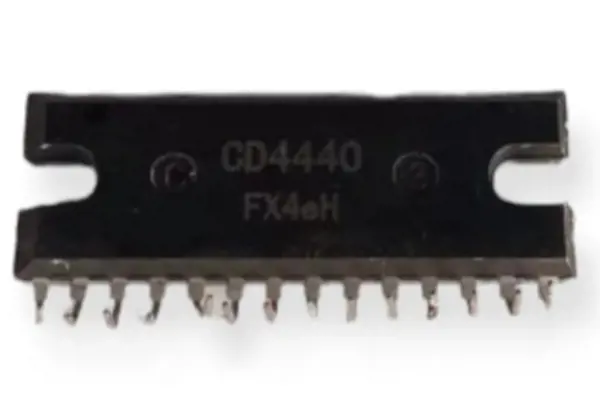
CD4440 IC: Datasheet...
The CD4440 IC is a stereo audio power amplifier ...
-

Advantages and Disad...
Operational amplifiers, or op-amps, offer a host...
Hot Products
-
Infineon Technologies Corporation
150V Single N-Channel HEXFET Power MOSFET in a D2-...
-
-
-

-
-
-
-
-
-
-
-
-
-
Vishay General Semiconductor - Diodes Division
Trans Voltage Suppressor Diode, 300W, 15V V(RWM), ...
-
-
-
-
-
-
-
-
-
-
-

-
-
-
-
-
-
-
-
-
-
-
-
-
-
-
-
-
-
-
-
-
-
-
-
-
Popular Manufacturers