

Images are for reference only See Product Specifications
ON FDB52N20TM
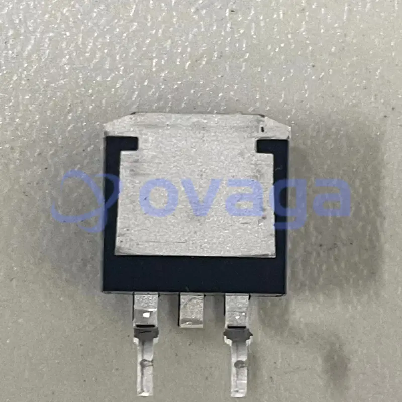
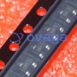
N-Channel 200 V 52A (Tc) 357W (Tc) Surface Mount TO-263 (D2PAK)


Brands: ON Semiconductor, LLC
Mfr.Part #: FDB52N20TM
Datasheet: FDB52N20TM Datasheet (PDF)
Package/Case: D2PAK
Product Type: Transistors
RoHS Status:
Stock Condition: 2756 pcs, New Original
Warranty: 1 Year Ovaga Warranty - Find Out More
0
1
Add To BomFDB52N20TM General Description
UniFETTM MOSFET is a high voltage MOSFET family based on planar stripe and DMOS technology. This MOSFET is tailored to reduce on-state resistance, and to provide better switching performance and higher avalanche energy strength. This device family is suitable for switching power converter applications such as power factor correction (PFC), flat panel display (FPD) TV power, ATX and electronic lamp ballasts.
Features
- RDS(on) = 49mΩ ( Max.)@ VGS = 10V, ID = 26A
- Low gate charge ( Typ. 49nC)
- Low Crss ( Typ. 66pF)
- 100% avalanche tested
Application
- This product is general usage and suitable for many different applications.
Specifications
| Parameter | Value | Parameter | Value |
|---|---|---|---|
| Source Content uid | FDB52N20TM | Pbfree Code | Yes |
| Part Life Cycle Code | Active | Ihs Manufacturer | ONSEMI |
| Package Description | D2PAK-3/2 | Manufacturer Package Code | 418AJ |
| Reach Compliance Code | not_compliant | ECCN Code | EAR99 |
| Factory Lead Time | 10 Weeks | Samacsys Manufacturer | onsemi |
| Avalanche Energy Rating (Eas) | 2520 mJ | Case Connection | DRAIN |
| Configuration | SINGLE WITH BUILT-IN DIODE | DS Breakdown Voltage-Min | 200 V |
| Drain Current-Max (ID) | 52 A | Drain-source On Resistance-Max | 0.049 Ω |
| FET Technology | METAL-OXIDE SEMICONDUCTOR | JEDEC-95 Code | TO-263 |
| JESD-30 Code | R-PSSO-G2 | JESD-609 Code | e3 |
| Moisture Sensitivity Level | 1 | Number of Elements | 1 |
| Number of Terminals | 2 | Operating Mode | ENHANCEMENT MODE |
| Operating Temperature-Max | 150 °C | Operating Temperature-Min | -55 °C |
| Package Body Material | PLASTIC/EPOXY | Package Shape | RECTANGULAR |
| Package Style | SMALL OUTLINE | Peak Reflow Temperature (Cel) | 245 |
| Polarity/Channel Type | N-CHANNEL | Power Dissipation-Max (Abs) | 357 W |
| Pulsed Drain Current-Max (IDM) | 208 A | Qualification Status | Not Qualified |
| Surface Mount | YES | Terminal Finish | Matte Tin (Sn) - annealed |
| Terminal Form | GULL WING | Terminal Position | SINGLE |
| Time@Peak Reflow Temperature-Max (s) | 30 | Transistor Application | SWITCHING |
| Transistor Element Material | SILICON | feature-category | Power MOSFET |
| feature-material | feature-process-technology | UniFET | |
| feature-configuration | Single | feature-channel-mode | Enhancement |
| feature-channel-type | N | feature-number-of-elements-per-chip | 1 |
| feature-maximum-drain-source-voltage-v | 200 | feature-maximum-gate-source-voltage-v | ±30 |
| feature-maximum-gate-threshold-voltage-v | feature-maximum-continuous-drain-current-a | 52 | |
| feature-maximum-drain-source-resistance-mohm | 49@10V | feature-typical-gate-charge-vgs-nc | 49@10V |
| feature-typical-gate-charge-10v-nc | 49 | feature-typical-input-capacitance-vds-pf | 2230@25V |
| feature-typical-output-capacitance-pf | feature-maximum-power-dissipation-mw | 357000 | |
| feature-packaging | Tape and Reel | feature-rad-hard | |
| feature-pin-count | 3 | feature-supplier-package | D2PAK |
| feature-standard-package-name1 | TO-263 | feature-cecc-qualified | No |
| feature-esd-protection | feature-military | No | |
| feature-aec-qualified | No | feature-aec-qualified-number | |
| feature-auto-motive | No | feature-p-pap | No |
| feature-eccn-code | EAR99 | feature-svhc | Yes |
| feature-svhc-exceeds-threshold | Yes |
Shipping
| Shipping Type | Ship Fee | Lead Time | |
|---|---|---|---|
 |
DHL | $20.00-$40.00 (0.50 KG) | 2-5 days |
 |
Fedex | $20.00-$40.00 (0.50 KG) | 2-5 days |
 |
UPS | $20.00-$40.00 (0.50 KG) | 2-5 days |
 |
TNT | $20.00-$40.00 (0.50 KG) | 2-5 days |
 |
EMS | $20.00-$40.00 (0.50 KG) | 2-5 days |
 |
REGISTERED AIR MAIL | $20.00-$40.00 (0.50 KG) | 2-5 days |
Processing Time:Shipping fee depend on different zone and country.
Payment
| Terms of payment | Hand Fee | |
|---|---|---|
 |
Wire Transfer | charge US$30.00 banking fee. |
 |
Paypal | charge 4.0% service fee. |
 |
Credit Card | charge 3.5% service fee. |
 |
Western Union | charge US.00 banking fee. |
 |
Money Gram | charge US$0.00 banking fee. |
Guarantees
1.The electronic components you purchase include 365 Days Warranty, We guarantee product quality.
2.If some of the items you received aren't of perfect quality, we would resiponsibly arrange your refund or replacement. But the items must remain their orginal condition.
Packing
-

Step1 :Product
-

Step2 :Vacuum packaging
-

Step3 :Anti-static bag
-

Step4 :Individual packaging
-

Step5 :Packaging boxes
-

Step6 :bar-code shipping tag


All the products will packing in anti-staticbag. Ship with ESD antistatic protection.
Outside ESD packing’s lable will use ourcompany’s information: Part Mumber, Brand and Quantity.
We will inspect all the goods before shipment,ensure all the products at good condition and ensure the parts are new originalmatch datasheet.
After all the goods are ensure no problems afterpacking, we will packing safely and send by global express. It exhibitsexcellent puncture and tear resistance along with good seal integrity.


Part points
-
The FDB52N20TM is a power MOSFET chip designed for various electronic applications. It has a high voltage rating of 200V and a continuous drain current of 52A, making it suitable for power switch devices. The chip features low on-resistance and fast switching capabilities, providing efficient power conversion. Its compact size and durability make it an ideal choice for automotive, industrial, and consumer electronics.
-
Equivalent
Some equivalent products of the FDB52N20TM chip are the IRFP250N and the IRFB11N50A. -
Features
The features of FDB52N20TM include N-channel MOSFET technology, a drain-source voltage of 200V, a continuous drain current of 52A, a low on-state resistance of 36mΩ, and a fast switching speed. It is suitable for various applications, including power supplies, motor drives, and inverters. -
Pinout
The FDB52N20TM is a MOSFET transistor with a TO-263 package, consisting of 3 pins. Pin 1 is the gate, pin 2 is the drain, and pin 3 is the source. It is commonly used in power electronic applications due to its high voltage and current handling capabilities. -
Manufacturer
The manufacturer of the FDB52N20TM is Fairchild Semiconductor. It is an American company that specializes in the design, development, and manufacturing of power management solutions. It offers a wide range of products including discrete semiconductors, integrated circuits, and optoelectronics for various industries such as automotive, industrial, and telecommunication. -
Application Field
The FDB52N20TM transistor is commonly used in various applications such as motor control, power supplies, and audio amplifier circuits. Additionally, it is suitable for use in high-speed switching applications due to its low resistance and fast-switching capability. -
Package
The FDB52N20TM chip is available in TO-263 package type. It has a form of a flat, rectangular shape with three leads. The size dimensions of the package are typically around 10mm x 10mm x 2mm.


Datasheet PDF
We provide high quality products, thoughtful service and after sale guarantee
-

We have rich products, can meet your various needs.
-

Minimum order quantity starts from 1pcs.
-

Lowest international shipping fee starts from $0.00
-

365 days quality guarantee for all products


Ovaga's components helped me create a product that impressed my clients.