


Images are for reference only See Product Specifications
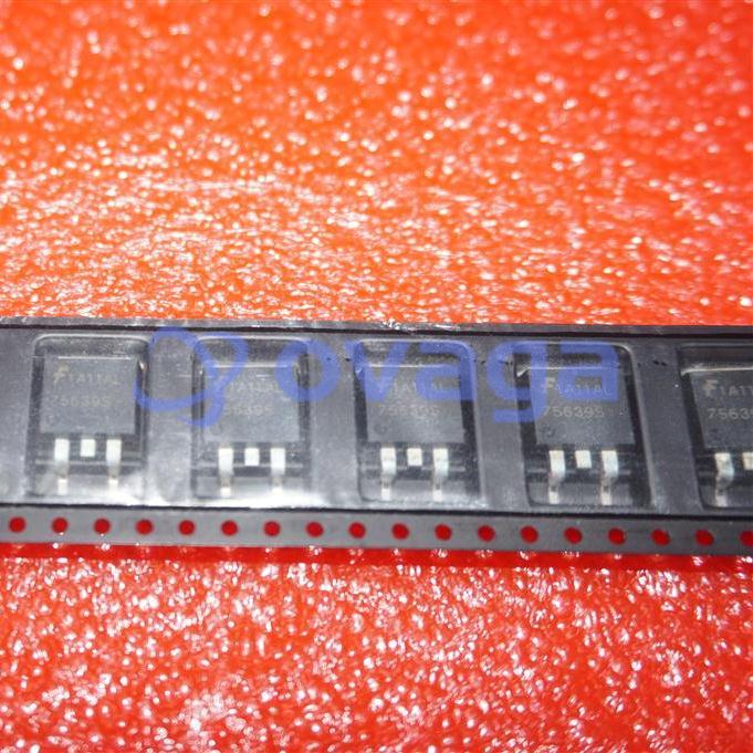
ON FDS2670
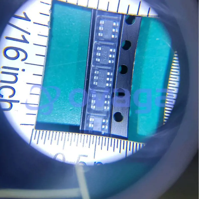
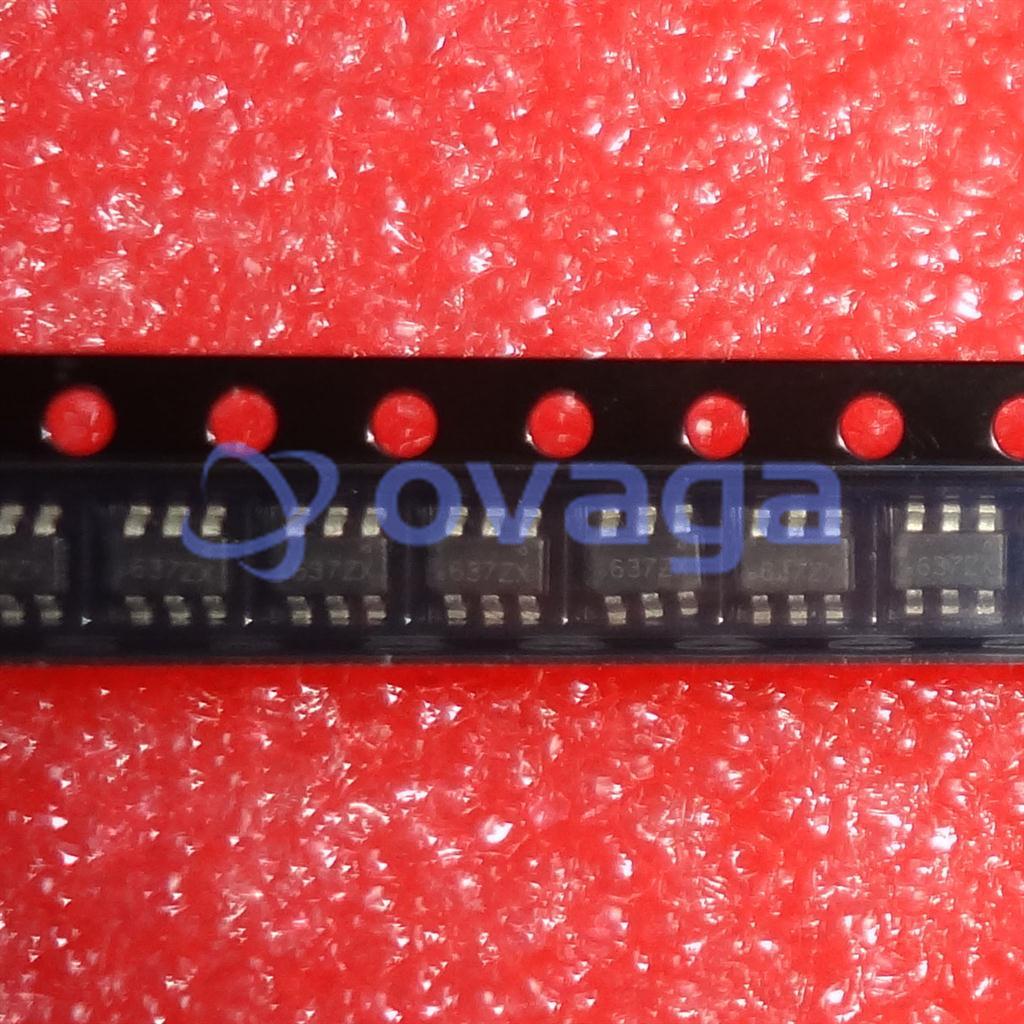
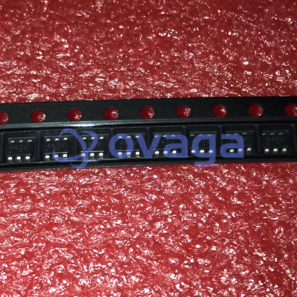
N-Channel 200 V 3A (Ta) 2.5W (Ta) Surface Mount 8-SOIC


Brands: ON Semiconductor, LLC
Mfr.Part #: FDS2670
Datasheet: FDS2670 Datasheet (PDF)
Package/Case: SOP-8
Product Type: Transistors
FDS2670 General Description
This N-Channel MOSFET has been designed specifically to improve the overall efficiency of DC/DC converters using either synchronous or conventional switching PWM controllers. These MOSFETs feature faster switching and lower gate charge than other MOSFETs with comparable RDS(ON) specifications. The result is a MOSFET that is easy and safer to drive (even at very high frequencies), and DC/DC power supply designs with higher overall efficiency.
Features
- 3.0A, 200 V
- RDS(ON) = 130 mΩ @ VGS = 10 V
- Low gate charge
- Fast switching speed
- High performance trench technology for extremely low RDS(ON)
- High power and current handling capability
Application
- This product is general usage and suitable for many different applications.
Specifications
| Parameter | Value | Parameter | Value |
|---|---|---|---|
| Source Content uid | FDS2670 | Pbfree Code | Yes |
| Part Life Cycle Code | Active | Ihs Manufacturer | ONSEMI |
| Package Description | SOIC-8 | Manufacturer Package Code | 751EB |
| Reach Compliance Code | compliant | ECCN Code | EAR99 |
| Factory Lead Time | 4 Weeks | Samacsys Manufacturer | onsemi |
| Configuration | SINGLE WITH BUILT-IN DIODE | DS Breakdown Voltage-Min | 200 V |
| Drain Current-Max (ID) | 3 A | Drain-source On Resistance-Max | 0.13 Ω |
| FET Technology | METAL-OXIDE SEMICONDUCTOR | JESD-30 Code | R-PDSO-G8 |
| JESD-609 Code | e3 | Moisture Sensitivity Level | 1 |
| Number of Elements | 1 | Number of Terminals | 8 |
| Operating Mode | ENHANCEMENT MODE | Operating Temperature-Max | 150 °C |
| Package Body Material | PLASTIC/EPOXY | Package Shape | RECTANGULAR |
| Package Style | SMALL OUTLINE | Peak Reflow Temperature (Cel) | 260 |
| Polarity/Channel Type | N-CHANNEL | Power Dissipation-Max (Abs) | 2.5 W |
| Qualification Status | Not Qualified | Surface Mount | YES |
| Terminal Finish | MATTE TIN | Terminal Form | GULL WING |
| Terminal Position | DUAL | Time@Peak Reflow Temperature-Max (s) | 30 |
| Transistor Application | SWITCHING | Transistor Element Material | SILICON |
| feature-category | Power MOSFET | feature-material | |
| feature-process-technology | PowerTrench | feature-configuration | Single Quad Drain Triple Source |
| feature-channel-mode | Enhancement | feature-channel-type | N |
| feature-number-of-elements-per-chip | 1 | feature-maximum-drain-source-voltage-v | 200 |
| feature-maximum-gate-source-voltage-v | ±20 | feature-maximum-gate-threshold-voltage-v | 4.5 |
| feature-maximum-continuous-drain-current-a | 3 | feature-maximum-drain-source-resistance-mohm | 130@10V |
| feature-typical-gate-charge-vgs-nc | 27@10V | feature-typical-gate-charge-10v-nc | 27 |
| feature-typical-input-capacitance-vds-pf | 1228@100V | feature-typical-output-capacitance-pf | 112 |
| feature-maximum-power-dissipation-mw | 2500 | feature-packaging | Tape and Reel |
| feature-rad-hard | feature-pin-count | 8 | |
| feature-supplier-package | SOIC | feature-standard-package-name1 | SO |
| feature-cecc-qualified | No | feature-esd-protection | |
| feature-military | No | feature-aec-qualified | No |
| feature-aec-qualified-number | feature-auto-motive | No | |
| feature-p-pap | No | feature-eccn-code | EAR99 |
| feature-svhc | No |
Shipping
| Shipping Type | Ship Fee | Lead Time | |
|---|---|---|---|
 |
DHL | $20.00-$40.00 (0.50 KG) | 2-5 days |
 |
Fedex | $20.00-$40.00 (0.50 KG) | 2-5 days |
 |
UPS | $20.00-$40.00 (0.50 KG) | 2-5 days |
 |
TNT | $20.00-$40.00 (0.50 KG) | 2-5 days |
 |
EMS | $20.00-$40.00 (0.50 KG) | 2-5 days |
 |
REGISTERED AIR MAIL | $20.00-$40.00 (0.50 KG) | 2-5 days |
Processing Time:Shipping fee depend on different zone and country.
Payment
| Terms of payment | Hand Fee | |
|---|---|---|
 |
Wire Transfer | charge US$30.00 banking fee. |
 |
Paypal | charge 4.0% service fee. |
 |
Credit Card | charge 3.5% service fee. |
 |
Western Union | charge US.00 banking fee. |
 |
Money Gram | charge US$0.00 banking fee. |
Guarantees
1.The electronic components you purchase include 365 Days Warranty, We guarantee product quality.
2.If some of the items you received aren't of perfect quality, we would resiponsibly arrange your refund or replacement. But the items must remain their orginal condition.
Packing
-

Step1 :Product
-

Step2 :Vacuum packaging
-

Step3 :Anti-static bag
-

Step4 :Individual packaging
-

Step5 :Packaging boxes
-

Step6 :bar-code shipping tag
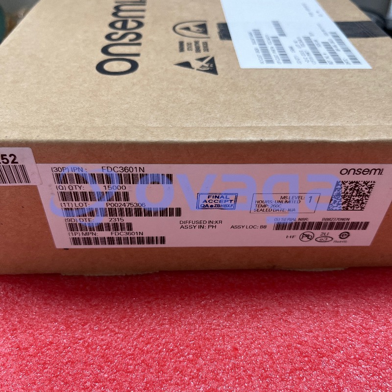
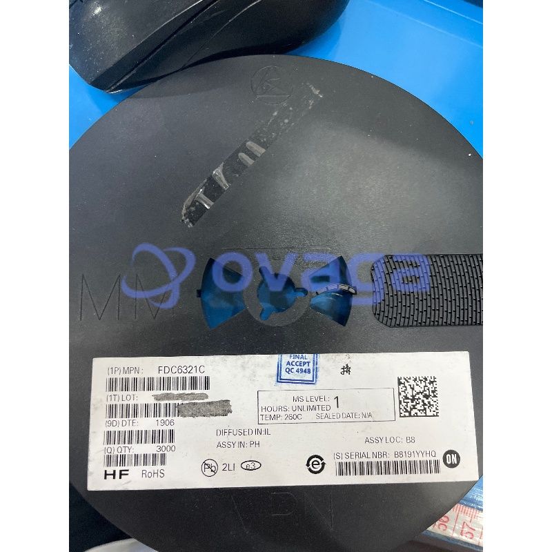
All the products will packing in anti-staticbag. Ship with ESD antistatic protection.
Outside ESD packing’s lable will use ourcompany’s information: Part Mumber, Brand and Quantity.
We will inspect all the goods before shipment,ensure all the products at good condition and ensure the parts are new originalmatch datasheet.
After all the goods are ensure no problems afterpacking, we will packing safely and send by global express. It exhibitsexcellent puncture and tear resistance along with good seal integrity.


Part points
-
The FDS2670 chip is an integrated circuit that combines a power MOSFET and a PWM controller into a single device. It is commonly used in applications such as power management, motor control, and battery charging. The chip offers a compact and efficient solution for driving high-current loads, providing improved performance and reliability.
-
Features
The FDS2670 is a power MOSFET transistor with a high current rating of 57A, low on-resistance of 0.03 ohms, and a low gate charge of 22nC. It is designed for high-performance switching applications, offering efficient power delivery and reliable operation. -
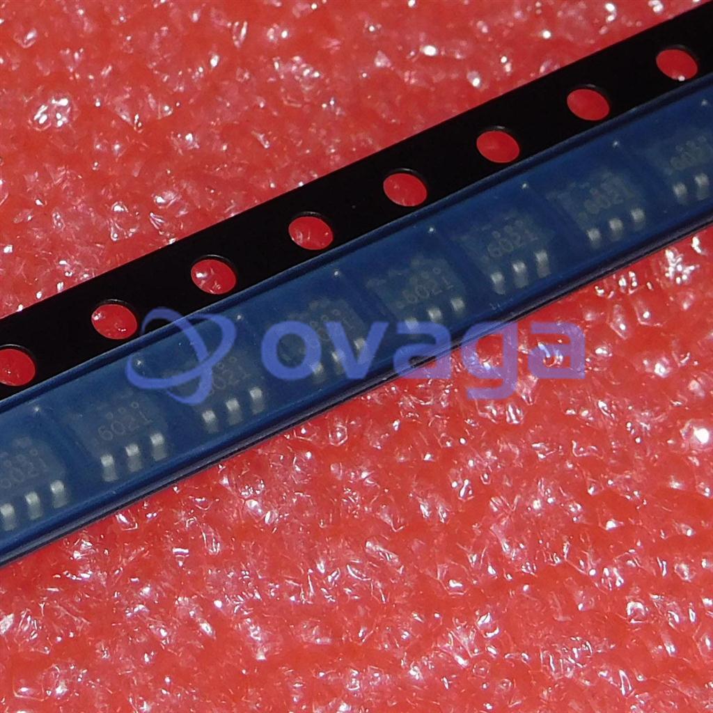
Pinout
The FDS2670 is a dual N-channel MOSFET with a small pin count. It typically has 8 pins, including the gate, source, and drain pins for each of its two channels. The function of this device is to switch and control electrical current in electronic circuits. -
Manufacturer
The manufacturer of the FDS2670 is Fairchild Semiconductor. Fairchild Semiconductor is a multinational company that specializes in the design, development, and manufacturing of high-performance semiconductor products. They provide a wide range of solutions for markets including automotive, consumer electronics, industrial, and telecommunications. -
Application Field
The FDS2670 MOSFET can be used in various application areas, including power management, motor control, and switching applications. It is commonly used in portable devices, automotive electronics, and industrial control systems. -
Package
The FDS2670 chip has a package type of Power33, a form of SO-8, and a size of 5.0mm x 4.5mm.
Datasheet PDF
We provide high quality products, thoughtful service and after sale guarantee
-

We have rich products, can meet your various needs.
-

Minimum order quantity starts from 1pcs.
-

Lowest international shipping fee starts from $0.00
-

365 days quality guarantee for all products
Components worked, but quality felt below average.