74HC164 vs 74HC595
Update Time: Nov 16, 2023 Readership: 774
Contents
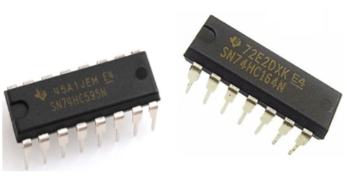
The 74HC164 and 74HC595 are both integrated circuits used in digital electronics, specifically categorized as 8-bit shift registers. Despite sharing this fundamental classification, they differ significantly in features and applications. The 74HC164 is a basic serial-in, parallel-out shift register, known for its simplicity and effectiveness in expanding digital outputs with minimal hardware. The 74HC595, on the other hand, is more sophisticated, offering additional functionalities such as an 8-bit storage register, output latches, and an output enable pin, enhancing its capability for more complex applications.
74HC164 Description
The 74HC164 is a popular integrated circuit (IC) that belongs to the 74HC series of high-speed CMOS (Complementary Metal-Oxide-Semiconductor) logic devices. Specifically, it is a 8-bit serial-in/parallel-out shift register. The "74" in its name indicates that it is a part of the 7400 series, and "HC" indicates that it is a high-speed CMOS version.
Features
-
Serial Input (DS)
This is where you input your data bit by bit. The 74HC164 shifts the bits in serially, from the DS pin to the first output (Q0), then to Q1, and so on.
-
Clock Input (SH_CP)
The clock input is used to synchronize the shifting of data. Each time a clock pulse is applied, the data at the serial input is shifted into the shift register.
-
Master Reset (MR)
This pin resets the shift register. When MR is taken low, it resets the internal state of the shift register, clearing all stored data.
-
Parallel Outputs (Q0 - Q7)
74HC164 Pinout
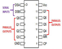
These are the parallel outputs of the shift register. The shifted-in data appears at these outputs after the appropriate number of clock pulses.
The 74HC164 is often used in applications where you need to expand the number of outputs from a microcontroller or other digital device. By serially shifting in data and then latching it to the parallel outputs, you can control multiple devices using only a few pins on your microcontroller.
The timing diagram for the 74HC164 is relatively straightforward. On each rising edge of the clock signal, the data at the serial input is shifted into the first bit, and the existing bits are shifted to the next stage. The process continues until all 8 bits are loaded, and then they can be latched to the parallel outputs.
74HC595 Description
The 74HC595 is a versatile 8-bit shift register, well-suited for applications requiring serial input to parallel output conversion. The 74HC595 shift register operates through a well-coordinated process involving data input, buffering, and output control.
Initially, data enters serially at the rising edge of the Serial Clock (SCK) through the Serial Data Load (SDL), getting stored in the internal 8-bit shift register. This data is then accessible via the Q7' output, allowing for continuous shifting without impacting the parallel output.
In the next phase, the Latch Clock (LCK) triggers at its rising edge, transferring the shift register's data into an 8-bit parallel output buffer, effectively updating the parallel output.
Finally, the Output Enable (OE) plays a crucial role in output management: when OE is low, the parallel output actively reflects the buffer’s content; a high OE, conversely, disables the output, shifting the parallel output terminals to a high-impedance state, thus safeguarding against any unintended signal disturbances. This orchestrated mechanism ensures efficient data handling and output control in the 74HC595.
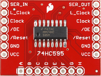
74HC595 Pinout
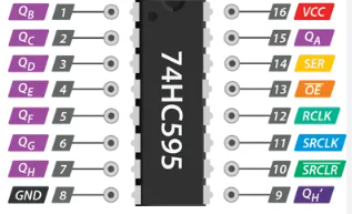
Working Principles of 74HC595
-
Data Terminals
QA-QH: Controls 8 segments of a digital display through eight-bit parallel output.
QH’: Cascade output terminal, connectable to another 595's SI (Serial Input) for expansion.
SI: Serial data input terminal.
-
Control Terminals
/SCLR (Pin 10): Clears shift register data when low. Typically connected to Vcc (positive voltage supply).
SCK (Pin 11): Shifts data at the rising edge; maintains at the falling edge. Suitable pulse width is in microseconds.
-
Control Shift Register
Data shifts at SCK's rising edge and holds at the falling edge.
-
Control Storage Register
Data transfers from the shift register to the storage register at RCK's rising edge, remaining stable at the falling edge.
/G (Pin 13): Disables output at a high level (high-impedance state). This control can prevent flickering and is more efficient than data end shift control.
Comparison with 74HC164
Functionality: Both 74HC164 and 74HC595 are 8-bit serial-to-parallel shift registers, but the 74HC595 has a higher drive current (35mA compared to 25mA for the 74HC164) and additional features.
Data Storage Register: The 74HC595's storage register ensures output stability during shifting, preventing flickering in slow serial transmissions.
Output Control: Unlike the 74HC164, which only has a data clearing terminal, the 74HC595 also includes an OE terminal, enabling high-impedance output states for more convenient usage.
Separate Clocks for Shift Register and Memory: The 74HC595 allows separate clock inputs for the shift register (SHcp) and storage register (STcp), offering precise control over data transfer and output.
Three-State Output Functionality: The 74HC595 supports a three-state bus output, enhancing its versatility in various circuit configurations.
74HC164 vs 74HC595
The 74HC595 excels in scenarios requiring speed, low voltage, and precise control over output changes, while the 74HC164 is well-suited for applications that benefit from simplicity, rapid updates to the output, and asynchronous reset functionality. The choice between them depends on the specific requirements of the application.
|
Feature |
74HC595 |
74HC164 |
|
Functional Design |
8-bit shift register with storage & output latches. |
Simpler 8-bit shift register. |
|
Output Control |
Storage register & OE pin for output control. |
Outputs are always active, no OE pin. |
|
Data Transfer |
Serial output pin (Q7’) for daisy-chaining. |
No serial output for cascading. |
|
Applications |
Suitable for complex tasks like driving LED displays. |
Better for basic tasks like simple LED control. |
|
Speed & Voltage |
Higher speed, lower voltage operation. |
Lower speed, higher voltage operation. |
|
Latch Functionality |
Has a latch for stable output. |
No latch, output changes with each clock. |
|
Cascade Configuration |
Dedicated Q7’ pin for cascading. |
Uses standard output pin Q7 for cascading. |
|
Reset Functionality |
Synchronous reset for shift register. |
Asynchronous reset. |
|
Data Buffering |
Prevents LED flashing during shifts. |
No buffering, potential LED flashing. |
-
Functional Differences
74HC595: This is an 8-bit shift register with a storage register and output latches. It allows serial to parallel conversion with the added feature of an 8-bit storage register that captures a snapshot of the shift register's contents on a clock input. This means that the 74HC595 can update its outputs without affecting the ongoing data shifting.
74HC164: The 74HC164 is a simpler 8-bit serial-in, parallel-out shift register. It doesn't have the additional storage register or output latches. The output of this shift register directly reflects the current contents of its internal flip-flops.
-
Output Control
74HC595: Offers more control over its outputs thanks to the storage register and the output enable (OE) pin. The OE pin can be used to disable all outputs simultaneously, providing flexibility in managing the output state.
74HC164: Lacks an output enable function, meaning its outputs are always active as long as the device is powered.
-
Data Transfer
74HC595: In addition to the serial input, it also features a serial output pin (Q7’), allowing multiple 74HC595s to be daisy-chained. This serial out feature provides an easy way to expand the number of outputs using multiple chips.
74HC164: It does not offer a serial output for cascading, making it less suitable for applications requiring many outputs.
-
Applications
74HC595: Commonly used in applications where data needs to be converted from serial to parallel format, such as driving LED displays, digital input expansion, etc. Its ability to latch output data makes it suitable for applications where output stability is crucial during data shifting.
74HC164: Better suited for simpler applications where a basic shift register is needed, and the lack of output latches is not a problem. It’s often used in basic LED control, simple logic circuits, etc.
-
Power Consumption
Both ICs are part of the high-speed CMOS family and have similar power consumption and speed characteristics. However, the specific requirements of your application, such as how fast the data shifts or the operating voltage, might make one more suitable than the other.
In summary, while both the 74HC595 and 74HC164 are useful as 8-bit shift registers, the 74HC595 offers additional features like a storage register, output enable, and daisy-chaining capability, making it more versatile for complex applications. The 74HC164, on the other hand, is more straightforward and suited for simpler, more direct applications.
-
Speed and Voltage
The 74HC595 operates at higher speeds and can function at lower voltages compared to the 74HC164, making it more versatile in different electronic environments.
-
Latch Functionality
The presence of a latch in the 74HC595 allows for stable output during data shifts, as the output remains unchanged until new data is latched. This feature is absent in the 74HC164, resulting in its output changing with each shift clock.
-
Cascade Configuration
The 74HC595's dedicated Q7’ pin for cascading multiple chips is a distinct advantage for expanding output capabilities without complicating the circuit. The 74HC164, however, uses its standard output pin Q7 for cascading, which is simpler but less flexible.
-
Output Enable (OE) Pin
The OE pin in the 74HC595 adds control over the output states, allowing outputs to be set to high impedance when needed. This feature is not available in the 74HC164, limiting its output control capabilities.
-
Reset Functionality
The 74HC595's synchronous reset affects the shift register, while resetting the latch register requires an additional step. The 74HC164's asynchronous reset is more straightforward but offers less control.
-
Additional Chip Compatibility
The 74HC164's compatibility with the 74HC165, a parallel-to-serial chip, adds versatility to its application in different circuit configurations.
-
Data Buffering
The absence of data buffering in the 74HC164 leads to potential LED flashing during data shifts, while the 74HC595's internal buffering prevents this, making it more suitable for applications where visual stability is important.
Final Words
The choice between the 74HC164 and 74HC595 depends largely on the application. The 74HC164, with its straightforward design, is ideal for simple applications that require basic serial-to-parallel data conversion, such as LED control or expanding digital outputs of microcontrollers. The 74HC595, in contrast, is better suited for more advanced applications where additional control and stability are needed. Its storage register and output latches provide more flexibility in data handling and output control, making it particularly useful in scenarios where data integrity during shifting is critical, such as driving sophisticated LED displays or complex digital interfaces.
Read More:
https://www.ovaga.com/products/detail/74hc164
https://www.ovaga.com/blog/transistor/74hc-vs-74ls-series-ics
Extended Reading
 FAQ
FAQ
-
Which is the most widely used shift register?
PISO or SIPO Shift Registers
-
What is the output of 74HC595?
The 74HC595 shift register is known for its 3-state outputs, which provide a unique and versatile functionality in digital electronics, especially when used with microcontrollers like the Arduino.
-
What is a 74HC164 shift register?
The 74HC164 and its variant, the 74HCT164, are types of digital shift registers. Essentially, these devices are 8-bit serial-in/parallel-out shift registers, meaning they can convert serial data input into parallel data output.
-
What are 74HC595 shift registers?
The 74HC595 is a type of shift register, which is a device used in digital electronics for the purpose of data storage or transfer. Specifically, the 74HC595 is a Serial-In/Parallel-Out (SIPO) shift register.
-
What is the difference between 74HC595 and 74HC165?
74HC165 is used for reading multiple digital inputs with fewer pins (PISO), while the 74HC595 is used for controlling multiple digital outputs with fewer pins (SIPO). This makes them complementary in nature for expanding the input and output capabilities of microcontroller systems.
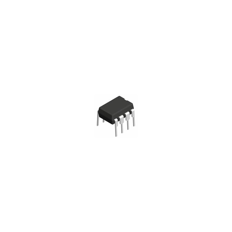
74HC164 8-Bit, Edge-triggered Shift Register In Stock: Pcs
Popular Blogs
-
PCA9617ADPJ Datashee...
The PCA9617ADPJ is a signal buffer and repeater ...
-
D882 Transistor Pino...
The D882 transistor is a commonly used NPN bipol...
-
C1815 Transistor Dat...
The C1815 is a general purpose NPN transistor us...
-
C945 Transistor Data...
The C945 transistor is a small, low-power NPN bi...
Hot Products

Popular Manufacturers