Images are for reference only See Product Specifications
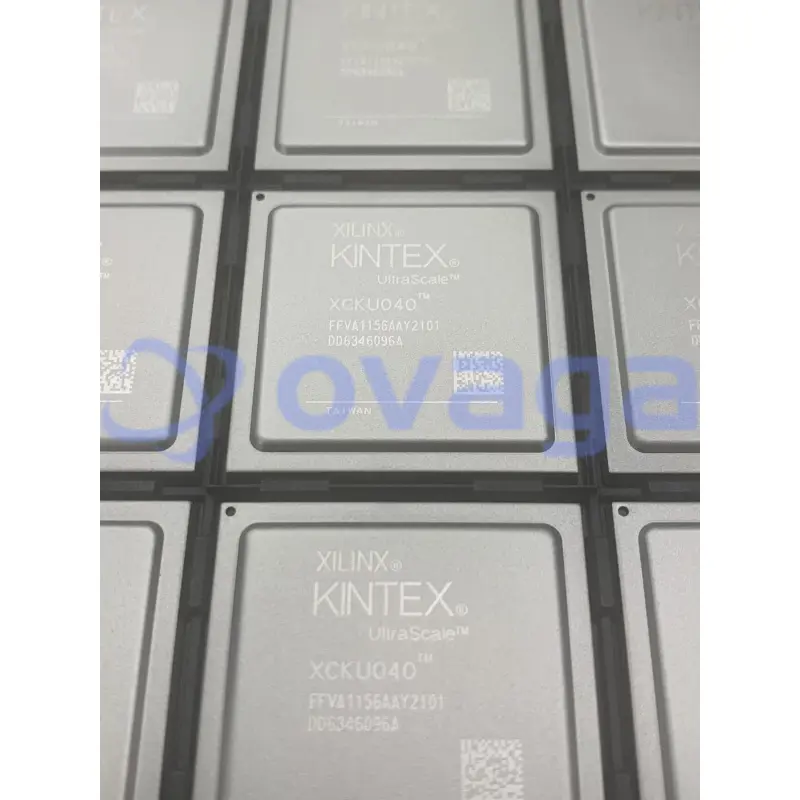
Xilinx XCKU040-2FFVA1156E
FPGA XCKU040 Family


Brands: Xilinx
Mfr.Part #: XCKU040-2FFVA1156E
Datasheet: XCKU040-2FFVA1156E Datasheet (PDF)
Package/Case: FCBGA-1156
Product Type: Programmable Logic ICs
RoHS Status:
Stock Condition: 2454 pcs, New Original
Warranty: 1 Year Ovaga Warranty - Find Out More
0
1
Add To BomXCKU040-2FFVA1156E General Description
The Xilinx XCKU040-2FFVA1156E is a member of the Virtex UltraScale+ family of field-programmable gate arrays (FPGAs). It features 240 I/O (input/output) pins, with a 1.8V core voltage and 3.3V I/O voltage. The device is based on a 16nm process technology and offers a combination of high performance, low power consumption, and high integration.This FPGA has a total of 486,720 logic cells, 780 DSP slices, and 19,040 KB of block RAM, providing users with ample resources for implementing complex designs. The device operates at a maximum frequency of 550MHz and can handle a wide range of applications, including high-speed data processing, wireless communications, automotive, and aerospace.The XCKU040-2FFVA1156E also includes features such as PCIe Gen3 x16, integrated IP blocks, advanced encryption capabilities, and multi-gigabit transceivers for high-speed serial communication. Additionally, the FPGA supports various industry-standard interfaces, such as HDMI, Gigabit Ethernet, USB, and DDR4 memory.
Features
- Series: Kintex UltraScale+
- Logic Cells: 363k
- RAM: 51.83Mb
- DSP Slices: 2940
- Transceivers: 32.5 Gb/s
- Speed Grade: -2
- Package: FFVA1156
- Operating Temperature: -40°C to 100°C
- Manufacturer: Xilinx
Application
- Telecommunications networking
- Medical imaging
- Industrial automation
- Aerospace and defense
- Automotive
- Video and image processing
- Data center applications
- High-performance computing
- Wireless communications
- Signal processing

Specifications
| Parameter | Value | Parameter | Value |
|---|---|---|---|
| Product Category | FPGA - Field Programmable Gate Array | RoHS | Details |
| Series | XCKU040 | Number of Logic Elements | 530250 LE |
| Adaptive Logic Modules - ALMs | 30300 ALM | Embedded Memory | 21.1 Mbit |
| Number of I/Os | 520 I/O | Supply Voltage - Min | 922 mV |
| Supply Voltage - Max | 979 mV | Minimum Operating Temperature | 0 C |
| Maximum Operating Temperature | + 100 C | Data Rate | 12.5 Gb/s |
| Number of Transceivers | 20 Transceiver | Mounting Style | SMD/SMT |
| Package / Case | FCBGA-1156 | Brand | Xilinx |
| Distributed RAM | 7 Mbit | Embedded Block RAM - EBR | 21.1 Mbit |
| Moisture Sensitive | Yes | Number of Logic Array Blocks - LABs | 30300 LAB |
| Operating Supply Voltage | 850 mV | Product Type | FPGA - Field Programmable Gate Array |
| Factory Pack Quantity | 1 | Subcategory | Programmable Logic ICs |
| Tradename | Kintex UltraScale |
Shipping
| Shipping Type | Ship Fee | Lead Time | |
|---|---|---|---|
 |
DHL | $20.00-$40.00 (0.50 KG) | 2-5 days |
 |
Fedex | $20.00-$40.00 (0.50 KG) | 2-5 days |
 |
UPS | $20.00-$40.00 (0.50 KG) | 2-5 days |
 |
TNT | $20.00-$40.00 (0.50 KG) | 2-5 days |
 |
EMS | $20.00-$40.00 (0.50 KG) | 2-5 days |
 |
REGISTERED AIR MAIL | $20.00-$40.00 (0.50 KG) | 2-5 days |
Processing Time:Shipping fee depend on different zone and country.
Payment
| Terms of payment | Hand Fee | |
|---|---|---|
 |
Wire Transfer | charge US$30.00 banking fee. |
 |
Paypal | charge 4.0% service fee. |
 |
Credit Card | charge 3.5% service fee. |
 |
Western Union | charge US.00 banking fee. |
 |
Money Gram | charge US$0.00 banking fee. |
Guarantees
1.The electronic components you purchase include 365 Days Warranty, We guarantee product quality.
2.If some of the items you received aren't of perfect quality, we would resiponsibly arrange your refund or replacement. But the items must remain their orginal condition.
Packing
-

Step1 :Product
-

Step2 :Vacuum packaging
-

Step3 :Anti-static bag
-

Step4 :Individual packaging
-

Step5 :Packaging boxes
-

Step6 :bar-code shipping tag


All the products will packing in anti-staticbag. Ship with ESD antistatic protection.
Outside ESD packing’s lable will use ourcompany’s information: Part Mumber, Brand and Quantity.
We will inspect all the goods before shipment,ensure all the products at good condition and ensure the parts are new originalmatch datasheet.
After all the goods are ensure no problems afterpacking, we will packing safely and send by global express. It exhibitsexcellent puncture and tear resistance along with good seal integrity.


Equivalent Parts
For the XCKU040-2FFVA1156E component, you may consider these replacement and alternative parts:
Part Number
Brands
Package
Description
Part Number : XCKU040-2FFVA1156E
Brands :
Package : 1156-BBGA, FCBGA
Description : There are no direct equivalent parts numbers for the XCKU040-2FFVA1156E as it is a unique FPGA from Xilinx. However, other FPGAs from Xilinx and other manufacturers may offer similar capabilities and can provide alternative options for specific applications.
Part points
-
The XCKU040-2FFVA1156E chip is a versatile field-programmable gate array (FPGA) that belongs to the Xilinx Kintex UltraScale family. It offers a high-performance and low-power solution for various applications, including data center, networking, and aerospace systems. With its advanced features like high-speed transceivers, configurable logic blocks, and embedded memory, the XCKU040-2FFVA1156E chip provides flexibility and scalability in hardware development.
-
Equivalent
There are no direct equivalent products to the XCKU040-2FFVA1156E chip. However, the Xilinx Virtex UltraScale+ family offers similar FPGA chips with varying features and specifications that may be suitable depending on the specific requirements of the application. -
Features
The features of XCKU040-2FFVA1156E include a Xilinx UltraScale+ FPGA, 965,000 logic cells, 5,520 DSP slices, 16.3 Mb of distributed RAM, 40 Mb of block RAM, 96 gigabit transceivers, and 65,520 CLB flip-flops. It also offers 640 digital I/O pins, PCIe Gen3 support, and up to 4.096 Mbits of integrated synchronous RAM. -
Pinout
The XCKU040-2FFVA1156E is a Field Programmable Gate Array (FPGA) with a pin count of 1156. The function of the FPGA can be customized according to user requirements, as it is programmable and can implement various digital logic functions. -
Manufacturer
The XCKU040-2FFVA1156E is manufactured by Xilinx Inc., a semiconductor company that specializes in the development and production of programmable logic devices and related software tools. -
Application Field
The XCKU040-2FFVA1156E is a Field Programmable Gate Array (FPGA) that can be used in various applications such as data center acceleration, wired communication, wireless infrastructure, industrial automation, and aerospace and defense. It offers high-performance computing, low-power capabilities, and advanced features for these application areas. -
Package
The XCKU040-2FFVA1156E chip is available in a Flip Chip Ball Grid Array (FCBGA) package type. It has a form factor of 1156 pins and a size of 35 mm x 35 mm.
Datasheet PDF
We provide high quality products, thoughtful service and after sale guarantee
-

We have rich products, can meet your various needs.
-

Minimum order quantity starts from 1pcs.
-

Lowest international shipping fee starts from $0.00
-

365 days quality guarantee for all products