Images are for reference only See Product Specifications
Orders Over
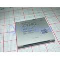
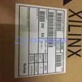
$5000Xilinx XC6SLX25-2FGG484I
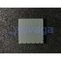
FPGA Cyclone® Family 4000 Cells 320.1MHz 130nm Technology 1.5V 400-Pin FBGA


Brands: Xilinx
Mfr.Part #: XC6SLX25-2FGG484I
Datasheet: XC6SLX25-2FGG484I Datasheet (PDF)
Package/Case: FCBGA-484
Product Type: FPGAs (Field Programmable Gate Array)
RoHS Status:
Stock Condition: 6,006 pcs, New Original
Warranty: 1 Year Ovaga Warranty - Find Out More
0
1
XC6SLX25-2FGG484I General Description
FPGA, SPARTAN-6 LX, 24K, 484FGGBGA; No. of Logic Blocks:3758; No. of Macrocells:24051; Family Type:Spartan-6; No. of Speed Grades:2; Total RAM Bits:958464; No. of I/O's:266; Clock Management:DCM, PLL; Core Supply Voltage Range:1.14V to 1.26V; I/O Supply Voltage:3.3V; Operating Frequency Max:33MHz; Operating Temperature Range:-40°C to +100°C; Logic Case Style:BGA; No. of Pins:484; MSL:MSL 3 - 168 hours; SVHC:No SVHC (19-Dec-2011)
Features
Spartan-6 Family:
Spartan-6 LX FPGA: Logic optimized
Spartan-6 LXT FPGA: High-speed serial connectivity
Designed for low cost
Multiple efficient integrated blocks
Optimized selection of I/O standards
Staggered pads
High-volume plastic wire-bonded packages
Low static and dynamic power
45 nm process optimized for cost and low power
Hibernate power-down mode for zero power
Suspend mode maintains state and configuration with
multi-pin wake-up, control enhancement
Lower-power 1.0V core voltage (LX FPGAs, -1L only)
High performance 1.2V core voltage (LX and LXT
FPGAs, -2, -3, and -4 speed grades)
Multi-voltage, multi-standard SelectIO interface banks
Up to 1,050 Mb/s data transfer rate per differential I/O
Selectable output drive, up to 24 mA per pin
3.3V to 1.2V I/O standards and protocols
Low-cost HSTL and SSTL memory interfaces
Hot swap compliance
Adjustable I/O slew rates to improve signal integrity
High-speed GTP serial transceivers in the LXT FPGAs
Up to 3.125 Gb/s
High-speed interfaces including: Serial ATA, Aurora,
1G Ethernet, PCI Express, OBSAI, CPRI, EPON, GPON, DisplayPort, and XAUI
Integrated Endpoint block for PCI Express designs (LXT)
Low-cost PCI technology support compatible with the 33 MHz, 32- and 64-bit specification.
Efficient DSP48A1 slices
High-performance arithmetic and signal processing
Fast 18 x 18 multiplier and 48-bit accumulator
Pipelining and cascading capability
Pre-adder to assist filter applications (Continue .)
Specifications
| Parameter | Value | Parameter | Value |
|---|---|---|---|
| Product Status | Active | Programmabe | Not Verified |
| Number of LABs/CLBs | 1879 | Number of Logic Elements/Cells | 24051 |
| Total RAM Bits | 958464 | Number of I/O | 266 |
| Number of Gates | - | Voltage - Supply | 1.14V ~ 1.26V |
| Mounting Type | Surface Mount | Operating Temperature | -40°C ~ 100°C (TJ) |
| Package / Case | 484-BBGA |
Shipping
| Shipping Type | Ship Fee | Lead Time | |
|---|---|---|---|
 |
DHL | $20.00-$40.00 (0.50 KG) | 2-5 days |
 |
Fedex | $20.00-$40.00 (0.50 KG) | 2-5 days |
 |
UPS | $20.00-$40.00 (0.50 KG) | 2-5 days |
 |
TNT | $20.00-$40.00 (0.50 KG) | 2-5 days |
 |
EMS | $20.00-$40.00 (0.50 KG) | 2-5 days |
 |
REGISTERED AIR MAIL | $20.00-$40.00 (0.50 KG) | 2-5 days |
Processing Time:Shipping fee depend on different zone and country.
Payment
| Terms of payment | Hand Fee | |
|---|---|---|
 |
Wire Transfer | charge US$30.00 banking fee. |
 |
Paypal | charge 4.0% service fee. |
 |
Credit Card | charge 3.5% service fee. |
 |
Western Union | charge US.00 banking fee. |
 |
Money Gram | charge US$0.00 banking fee. |
Guarantees
1.The electronic components you purchase include 365 Days Warranty, We guarantee product quality.
2.If some of the items you received aren't of perfect quality, we would resiponsibly arrange your refund or replacement. But the items must remain their orginal condition.
Packing
-

Step1 :Product
-

Step2 :Vacuum packaging
-

Step3 :Anti-static bag
-

Step4 :Individual packaging
-

Step5 :Packaging boxes
-

Step6 :bar-code shipping tag


All the products will packing in anti-staticbag. Ship with ESD antistatic protection.
Outside ESD packing’s lable will use ourcompany’s information: Part Mumber, Brand and Quantity.
We will inspect all the goods before shipment,ensure all the products at good condition and ensure the parts are new originalmatch datasheet.
After all the goods are ensure no problems afterpacking, we will packing safely and send by global express. It exhibitsexcellent puncture and tear resistance along with good seal integrity.


Part points
-
The XC6SLX25-2FGG484I chip is a Field-Programmable Gate Array (FPGA) from Xilinx. It offers 25,920 logic cells, 1,620 Kbits of block RAM, and 216 DSP slices. It operates at a speed grade of -2 and comes in a 484-pin fine-grid ball grid array (FGGBA) package. The chip is mainly used for digital logic implementation and can be configured or reprogrammed to fit specific application requirements.
-
Equivalent
The equivalent products of XC6SLX25-2FGG484I chip are Xilinx Spartan-6 LX Family and Spartan-6 FPGAs. -
Features
The features of XC6SLX25-2FGG484I include a Spartan-6 FPGA with 25,920 logic cells, 48 18kb block RAMs, 2 DSP slices, and 356 I/O pins. It has a maximum operating frequency of 400MHz and can operate with a 1.2V core voltage. It is packaged in a 484-pin Fine-Pitch Ball Grid Array (FBGA) package. -
Pinout
The XC6SLX25-2FGG484I is an FPGA (Field-Programmable Gate Array) device manufactured by Xilinx. It has a pin count of 484 and is from the Spartan-6 LX family. The specific pin functions and configuration options can be found in the datasheet provided by the manufacturer. -
Manufacturer
The manufacturer of the XC6SLX25-2FGG484I is Xilinx Inc. It is a leading American technology company specializing in the development and production of programmable logic devices and associated software tools. -
Application Field
The XC6SLX25-2FGG484I is a field-programmable gate array (FPGA) that can be used in various application areas, including aerospace and defense, automotive, industrial automation, telecommunications, and scientific research. Its high-performance capabilities and flexibility make it suitable for a wide range of applications requiring complex digital logic and signal processing functions. -
Package
The XC6SLX25-2FGG484I chip has a FBGA (Fine-Pitch Ball Grid Array) package type, a grid array form, and a size of 484 pins.


We provide high quality products, thoughtful service and after sale guarantee
-

We have rich products, can meet your various needs.
-

Minimum order quantity starts from 1pcs.
-

Lowest international shipping fee starts from $0.00
-

365 days quality guarantee for all products