Images are for reference only See Product Specifications
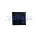
Xilinx XC5VLX50-3FFG676C
Virtex®-5 LX Field Programmable Gate Array (FPGA) IC 440 1769472 46080 676-BBGA, FCBGA


Brands: AMD Xilinx, Inc
Mfr.Part #: XC5VLX50-3FFG676C
Datasheet: XC5VLX50-3FFG676C Datasheet (PDF)
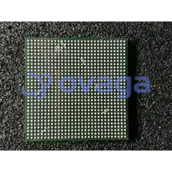
Package/Case: FCBGA-676
Product Type: Programmable Logic ICs
RoHS Status:
Stock Condition: 3624 pcs, New Original
Warranty: 1 Year Ovaga Warranty - Find Out More
0
1
Add To BomXC5VLX50-3FFG676C General Description
Virtex®-5 LX Field Programmable Gate Array (FPGA) IC 440 1769472 46080 676-BBGA, FCBGA
Features
- Logic Cells: 54,480
- Block RAM: 3,456 Kbits
- DSP Slices: 200
- Clock Management Tiles: 8
- Maximum User I/Os: 500
- Transceiver Count: 8
Application
- EP3SL150F1152C3N (Intel FPGA)
- A3P1000-2FGG676I (Microchip FPGA)
- LFXP10C-4F256C (Lattice Semiconductor FPGA)

Specifications
| Parameter | Value | Parameter | Value |
|---|---|---|---|
| Rohs Code | Yes | Part Life Cycle Code | Transferred |
| Ihs Manufacturer | XILINX INC | Part Package Code | BGA |
| Package Description | BGA-676 | Pin Count | 676 |
| Reach Compliance Code | compliant | ECCN Code | 3A991.D |
| HTS Code | 8542.39.00.01 | Factory Lead Time | 72 Weeks |
| Combinatorial Delay of a CLB-Max | 0.67 ns | JESD-30 Code | S-PBGA-B676 |
| JESD-609 Code | e1 | Length | 27 mm |
| Moisture Sensitivity Level | 4 | Number of CLBs | 3600 |
| Number of Inputs | 440 | Number of Logic Cells | 46080 |
| Number of Outputs | 440 | Number of Terminals | 676 |
| Operating Temperature-Max | 85 °C | Operating Temperature-Min | |
| Organization | 3600 CLBS | Package Body Material | PLASTIC/EPOXY |
| Package Code | BGA | Package Equivalence Code | BGA676,26X26,40 |
| Package Shape | SQUARE | Package Style | GRID ARRAY |
| Peak Reflow Temperature (Cel) | 250 | Programmable Logic Type | FIELD PROGRAMMABLE GATE ARRAY |
| Qualification Status | Not Qualified | Seated Height-Max | 3 mm |
| Supply Voltage-Max | 1.05 V | Supply Voltage-Min | 0.95 V |
| Supply Voltage-Nom | 1 V | Surface Mount | YES |
| Temperature Grade | OTHER | Terminal Finish | TIN SILVER COPPER |
| Terminal Form | BALL | Terminal Pitch | 1 mm |
| Terminal Position | BOTTOM | Time@Peak Reflow Temperature-Max (s) | 30 |
| Width | 27 mm |
Shipping
| Shipping Type | Ship Fee | Lead Time | |
|---|---|---|---|
 |
DHL | $20.00-$40.00 (0.50 KG) | 2-5 days |
 |
Fedex | $20.00-$40.00 (0.50 KG) | 2-5 days |
 |
UPS | $20.00-$40.00 (0.50 KG) | 2-5 days |
 |
TNT | $20.00-$40.00 (0.50 KG) | 2-5 days |
 |
EMS | $20.00-$40.00 (0.50 KG) | 2-5 days |
 |
REGISTERED AIR MAIL | $20.00-$40.00 (0.50 KG) | 2-5 days |
Processing Time:Shipping fee depend on different zone and country.
Payment
| Terms of payment | Hand Fee | |
|---|---|---|
 |
Wire Transfer | charge US$30.00 banking fee. |
 |
Paypal | charge 4.0% service fee. |
 |
Credit Card | charge 3.5% service fee. |
 |
Western Union | charge US.00 banking fee. |
 |
Money Gram | charge US$0.00 banking fee. |
Guarantees
1.The electronic components you purchase include 365 Days Warranty, We guarantee product quality.
2.If some of the items you received aren't of perfect quality, we would resiponsibly arrange your refund or replacement. But the items must remain their orginal condition.
Packing
-

Step1 :Product
-

Step2 :Vacuum packaging
-

Step3 :Anti-static bag
-

Step4 :Individual packaging
-

Step5 :Packaging boxes
-

Step6 :bar-code shipping tag


All the products will packing in anti-staticbag. Ship with ESD antistatic protection.
Outside ESD packing’s lable will use ourcompany’s information: Part Mumber, Brand and Quantity.
We will inspect all the goods before shipment,ensure all the products at good condition and ensure the parts are new originalmatch datasheet.
After all the goods are ensure no problems afterpacking, we will packing safely and send by global express. It exhibitsexcellent puncture and tear resistance along with good seal integrity.


Part points
-
The XC5VLX50-3FFG676C is a field-programmable gate array (FPGA) chip manufactured by Xilinx. It belongs to the Virtex-5 family and offers advanced features and high performance for various applications. The chip operates at a speed grade of -3 and has a package configuration of FF676. It is designed for use in demanding systems that require programmable logic solutions.
-
Equivalent
The equivalent products of the XC5VLX50-3FFG676C chip are the XC5VLX50-1FFG676C and XC5VLX50-2FFG676C chips from Xilinx's Virtex-5 LX FPGA series. -
Features
The XC5VLX50-3FFG676C is a Virtex-5 LX FPGA with a capacity of 50,615 logic cells, operating at a maximum speed of 550MHz. It has 36,864 distributed RAM bits and 640KB block RAM. Additionally, it provides 32 I/O standards, four clock management tiles, and supports embedded multipliers up to 25x18 bits. -
Pinout
The XC5VLX50-3FFG676C is a Field Programmable Gate Array (FPGA) with a pin count of 676. It is part of the Virtex-5 family by Xilinx and operates with a core voltage of 1.0V. The specific pin functions can be found in the datasheet provided by the manufacturer. -
Manufacturer
The manufacturer of the XC5VLX50-3FFG676C is Xilinx Inc. Xilinx is an American technology company specializing in the design and production of programmable logic devices and associated software. They are known for their field-programmable gate arrays (FPGAs) and provide solutions for a variety of industries such as telecommunications, automotive, aerospace, and data centers. -
Application Field
The XC5VLX50-3FFG676C is an FPGA (Field Programmable Gate Array) and can be used in various application areas such as telecommunications, networking, compute-intensive applications, video processing, industrial control systems, and high-performance computing. It is designed to provide high processing performance, flexibility, and scalability for a wide range of applications in these fields. -
Package
The XC5VLX50-3FFG676C chip is packaged in a FG676 package type, has a size of 27mm x 27mm, and is in a flip-chip form.
Datasheet PDF
We provide high quality products, thoughtful service and after sale guarantee
-

We have rich products, can meet your various needs.
-

Minimum order quantity starts from 1pcs.
-

Lowest international shipping fee starts from $0.00
-

365 days quality guarantee for all products