Images are for reference only See Product Specifications
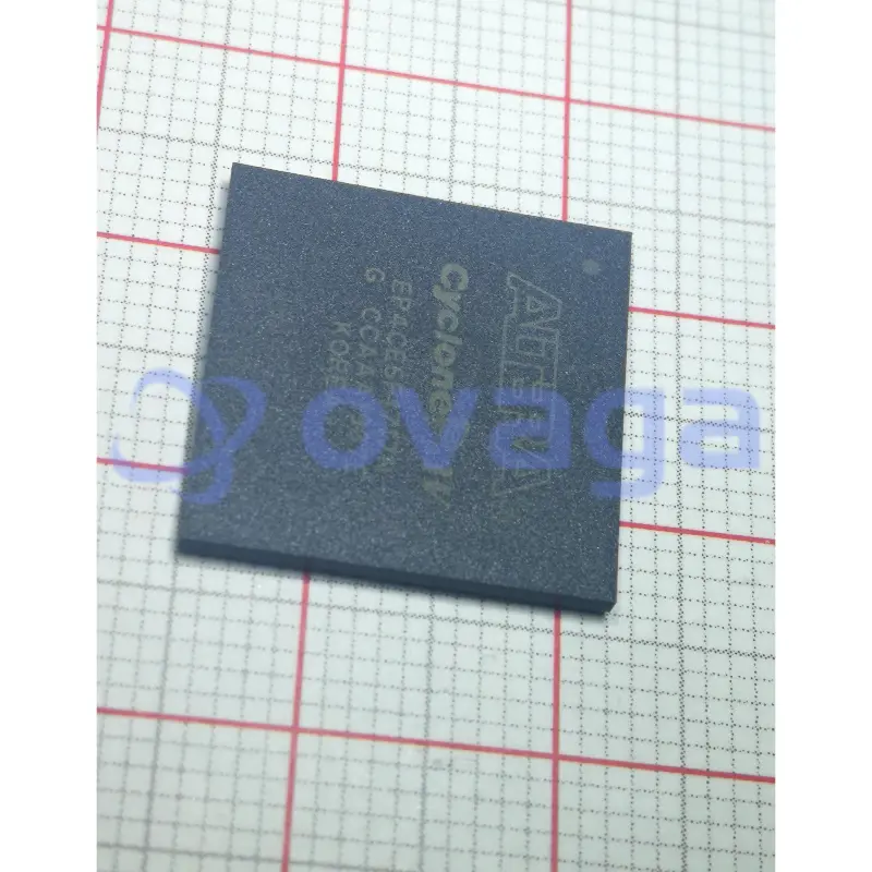
Altera EP3C25F324C7N
FPGA Cyclone® III Family 24624 Cells 437.5MHz 65nm Technology 1.2V 324-Pin FBGA


Brands: Altera Corporation (Intel)
Mfr.Part #: EP3C25F324C7N
Datasheet: EP3C25F324C7N Datasheet (PDF)
Package/Case: FBGA-324
Product Type: Programmable Logic ICs
EP3C25F324C7N General Description
Cyclone® III Field Programmable Gate Array (FPGA) IC 215 608256 24624 324-BGA
Features
- 25,408 logic elements (LEs)
- 504 embedded memory blocks (18-Kbit RAM blocks)
- 24 multipliers
- 4 PLLs (Phase Locked Loops)
- 316 user I/O pins
- Maximum operating frequency of 350MHz
Application
- Industrial automation and control systems
- Communications equipment
- Medical equipment
- Video and image processing systems
- Test and measurement equipment
- Military and aerospace applications
 Inventory")
Specifications
| Parameter | Value | Parameter | Value |
|---|---|---|---|
| feature-family-name | Cyclone® III | feature-process-technology | 65nm |
| feature-maximum-number-of-user-i-os | 215 | feature-number-of-registers | |
| feature-device-logic-cells | 24624 | feature-device-system-gates | |
| feature-number-of-multipliers | 66 (18x18) | feature-program-memory-type | SRAM |
| feature-ram-bits-kbit | 594 | feature-total-number-of-block-ram | 66 |
| feature-ethernet-macs | feature-supported-ip-core | 32/64-bit PCI-X bus Master/Target interface Core, 66/100/133Mhz|10 Gigabit Ethernet MAC|SpeedView Enabled JPEG Encoder (SVE-JPEG-E)|V1 ColdFire|Viterbi Compiler, Low-Speed/Hybrid Serial Decoder | |
| feature-supported-ip-core-manufacture | Altera/Freescale/CAST, Inc/MorethanIP/PLDA | feature-maximum-number-of-serdes-channels | |
| feature-device-logic-units | 24624 | feature-device-number-of-dlls-plls | 4 |
| feature-transceiver-blocks | feature-transceiver-speed-gbps | ||
| feature-dedicated-dsp | feature-pci-blocks | ||
| feature-programmability | No | feature-maximum-internal-frequency-mhz | 437.5 |
| feature-speed-grade | 7 | feature-giga-multiply-accumulates-per-second | |
| feature-differential-i-o-standards-supported | RSDS|SSTL-18|SSTL-2|HSTL-12|HSTL-15|HSTL-18|LVDS|LVPECL | feature-single-ended-i-o-standards-supported | HSTL|SSTL|PCI-X|PCI|LVCMOS|LVTTL |
| feature-external-memory-interface | QDRII+SRAM|DDR2 SDRAM | feature-minimum-operating-supply-voltage-v | 1.15 |
| feature-maximum-operating-supply-voltage-v | 1.25 | feature-packaging | |
| feature-rohs | feature-rad-hard | ||
| feature-pin-count | 324 | feature-supplier-package | FBGA |
| feature-standard-package-name1 | BGA | feature-cecc-qualified | No |
| feature-esd-protection | feature-escc-qualified | ||
| feature-military | No | feature-aec-qualified | No |
| feature-aec-qualified-number | feature-auto-motive | No | |
| feature-p-pap | No | feature-eccn-code | 3A991d. |
| feature-svhc | Yes |
Shipping
| Shipping Type | Ship Fee | Lead Time | |
|---|---|---|---|
 |
DHL | $20.00-$40.00 (0.50 KG) | 2-5 days |
 |
Fedex | $20.00-$40.00 (0.50 KG) | 2-5 days |
 |
UPS | $20.00-$40.00 (0.50 KG) | 2-5 days |
 |
TNT | $20.00-$40.00 (0.50 KG) | 2-5 days |
 |
EMS | $20.00-$40.00 (0.50 KG) | 2-5 days |
 |
REGISTERED AIR MAIL | $20.00-$40.00 (0.50 KG) | 2-5 days |
Processing Time:Shipping fee depend on different zone and country.
Payment
| Terms of payment | Hand Fee | |
|---|---|---|
 |
Wire Transfer | charge US$30.00 banking fee. |
 |
Paypal | charge 4.0% service fee. |
 |
Credit Card | charge 3.5% service fee. |
 |
Western Union | charge US.00 banking fee. |
 |
Money Gram | charge US$0.00 banking fee. |
Guarantees
1.The electronic components you purchase include 365 Days Warranty, We guarantee product quality.
2.If some of the items you received aren't of perfect quality, we would resiponsibly arrange your refund or replacement. But the items must remain their orginal condition.
Packing
-

Step1 :Product
-

Step2 :Vacuum packaging
-

Step3 :Anti-static bag
-

Step4 :Individual packaging
-

Step5 :Packaging boxes
-

Step6 :bar-code shipping tag
All the products will packing in anti-staticbag. Ship with ESD antistatic protection.
Outside ESD packing’s lable will use ourcompany’s information: Part Mumber, Brand and Quantity.
We will inspect all the goods before shipment,ensure all the products at good condition and ensure the parts are new originalmatch datasheet.
After all the goods are ensure no problems afterpacking, we will packing safely and send by global express. It exhibitsexcellent puncture and tear resistance along with good seal integrity.


Equivalent Parts
For the EP3C25F324C7N component, you may consider these replacement and alternative parts:
Part Number
Brands
Package
Description
Part Number : EP3C25F324I7N
Brands :
Package : FBGA-324
Description : FPGA Cyclone® III Family 24624 Cells 437.5MHz 65nm Technology 1.2V
Part Number : EP3C25F256C8N
Brands :
Package : FBGA-256
Description : FPGA Cyclone? III Family 24624 Cells 402MHz 65nm Technology 1.2V 256-Pin FBGA
Part Number : EP3C25U256C8N
Brands :
Package : BGA-256
Description : FPGA, CYCLONE III, 25K LE, 256UBGA Programmable Logic Type:FPGA; Logic IC function:FPGA; Logic IC family:Cyclone III; Logic IC Base Number:3; I/O lines, No. of:156;
Part Number : EP3C25U256I7N
Brands :
Package : BGA-256
Description : FPGA Cyclone III Family 24624 Cells 437.5MHz 65nm Technology 1.2V 256Pin UFBGA
Part Number : EP3C25Q240C8N
Brands :
Package : PQFP-240
Description : FPGA, CYCLONE III, 25K LE, 240PQFP
Part points
-
The EP3C25F324C7N is a field-programmable gate array (FPGA) chip from the Cyclone III family by Intel (formerly Altera). It offers 25,000 logic elements, 324 Kbits of embedded memory, and can run at speeds up to 300 MHz. It is used in industrial applications, communication systems, and embedded computing devices.
-
Equivalent
Some equivalent products to EP3C25F324C7N chip are Altera Cyclone III EP3C25F324C8N, Cyclone III EP3C25F324C7N, and EP3C25F324I7N. These chips may have slightly different specifications or features, but they are generally interchangeable for many applications. -
Features
The EP3C25F324C7N is a programmable logic device featuring 25,000 logic elements, 324 Kbits of embedded memory, and 288 I/O pins. It operates at a voltage range of 1.14V to 1.26V and supports various I/O standards such as LVCMOS, LVTTL, and SSTL. It also includes on-chip PLLs for clock management. -
Pinout
The EP3C25F324C7N has a 324-pin count and is a field-programmable gate array (FPGA) with 25,920 logic elements and 564 Kbits of embedded memory. It is designed for high-performance applications such as signal processing, communications, and industrial automation. -
Manufacturer
The EP3C25F324C7N is manufactured by Altera Corporation, a semiconductor company specializing in programmable logic devices. They are known for their FPGA (Field Programmable Gate Array) products that are widely used in various industries for custom hardware acceleration, signal processing, and other applications. -
Application Field
The EP3C25F324C7N is commonly used in industrial automation, automotive, telecommunications, medical devices, and consumer electronics applications. It is suitable for applications that require a combination of high performance, low power consumption, and flexibility in design. Its features make it well suited for a wide range of embedded systems and control applications. -
Package
The EP3C25F324C7N chip is available in a 324-pin FineLine BGA (FBGA) package type. It comes in a form of programmable logic device (PLD) and has a size of 17mm x 17mm.
Datasheet PDF
We provide high quality products, thoughtful service and after sale guarantee
-

We have rich products, can meet your various needs.
-

Minimum order quantity starts from 1pcs.
-

Lowest international shipping fee starts from $0.00
-

365 days quality guarantee for all products