
Images are for reference only See Product Specifications
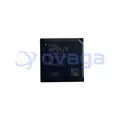
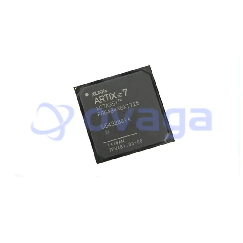
Xilinx XC7A35T-2FGG484I

Artix-7 Field Programmable Gate Array (FPGA) IC 250 1843200 33280 484-BBGA


Brands: AMD Xilinx, Inc
Mfr.Part #: XC7A35T-2FGG484I
Datasheet: XC7A35T-2FGG484I Datasheet (PDF)
Package/Case: 484-BBGA
RoHS Status:
Stock Condition: 3505 pcs, New Original
Product Type: Programmable Logic ICs
Warranty: 1 Year Ovaga Warranty - Find Out More
0
1
*All prices are in USD
| Qty | Unit Price | Ext Price |
|---|---|---|
| 1 | $22.592 | $22.592 |
| 10 | $19.416 | $194.160 |
| 60 | $17.978 | $1078.680 |
| 120 | $16.722 | $2006.640 |
In Stock:3505 PCS
XC7A35T-2FGG484I General Description
The XC7A35T-2FGG484I is a specific member of the Xilinx Artix-7 FPGA (Field-Programmable Gate Array) family. Xilinx provides a range of FPGAs with varying capacities and features to meet different application requirements.
Features
FPGA Family: Artix-7 is a family of FPGAs known for offering a balance of low power consumption, high performance, and high logic density. They are suitable for a wide range of applications.
Logic Cells: The "35T" in the part number indicates the number of logic cells in the FPGA. In this case, it has approximately 33,280 logic cells.
Speed Grade: The "-2" in the part number signifies the speed grade of the FPGA. Speed grades represent the maximum frequency at which the FPGA can operate reliably. A lower number is typically faster.
Package Type: The "FGG484" specifies the package type. "FGG" refers to a Fine-Pitch Ball Grid Array (BGA) package with 484 pins.
Industrial Temperature Grade: The "I" in the part number indicates that the device is rated for industrial temperature range.
Configuration: Artix-7 FPGAs support configuration from various sources, including configuration from an external flash memory.
Memory Resources: The FPGA includes on-chip memory resources, such as Block RAM (BRAM) and distributed RAM, which can be used for data storage and processing.
Clock Management: The FPGA provides built-in clock management resources, including PLLs (Phase-Locked Loops) for generating and managing clock signals.
I/O Interfaces: The "484" in the package code indicates the number of I/O pins available in the specific package. These pins can be configured for various purposes, including input, output, and bidirectional communication.Developers use Xilinx Vivado development tools to design, program, and configure these FPGAs for specific applications.
Application
Developers use Xilinx Vivado development tools to design, program, and configure these FPGAs for specific applications.

Specifications
| Parameter | Value | Parameter | Value |
|---|---|---|---|
| Product Name | XC7A35T-2FGG484I | Product Type | Field-Programmable Gate Array (FPGA) |
| Logic Cells | 33,280 | DSP Slices | 90 |
| Block RAM | 1,800 Kbits | Max User I/Os | 200 |
| Operating Frequency | Up to 600 MHz | Programmable Logic Cells | 6-input Look-Up Tables (LUTs) |
| Package | FGG484 | Supply Voltage Range | 1.0V, 1.2V, 1.5V, 1.8V, 2.5V, 3.3V |
| Operating Temperature Range | -40°C to 100°C |
Shipping
| Shipping Type | Ship Fee | Lead Time | |
|---|---|---|---|
 |
DHL | $20.00-$40.00 (0.50 KG) | 2-5 days |
 |
Fedex | $20.00-$40.00 (0.50 KG) | 2-5 days |
 |
UPS | $20.00-$40.00 (0.50 KG) | 2-5 days |
 |
TNT | $20.00-$40.00 (0.50 KG) | 2-5 days |
 |
EMS | $20.00-$40.00 (0.50 KG) | 2-5 days |
 |
REGISTERED AIR MAIL | $20.00-$40.00 (0.50 KG) | 2-5 days |
Processing Time:Shipping fee depend on different zone and country.
Payment
| Terms of payment | Hand Fee | |
|---|---|---|
 |
Wire Transfer | charge US$30.00 banking fee. |
 |
Paypal | charge 4.0% service fee. |
 |
Credit Card | charge 3.5% service fee. |
 |
Western Union | charge US.00 banking fee. |
 |
Money Gram | charge US$0.00 banking fee. |
Guarantees
1.The electronic components you purchase include 365 Days Warranty, We guarantee product quality.
2.If some of the items you received aren't of perfect quality, we would resiponsibly arrange your refund or replacement. But the items must remain their orginal condition.
Packing
-

Step1 :Product
-

Step2 :Vacuum packaging
-

Step3 :Anti-static bag
-

Step4 :Individual packaging
-

Step5 :Packaging boxes
-

Step6 :bar-code shipping tag


All the products will packing in anti-staticbag. Ship with ESD antistatic protection.
Outside ESD packing’s lable will use ourcompany’s information: Part Mumber, Brand and Quantity.
We will inspect all the goods before shipment,ensure all the products at good condition and ensure the parts are new originalmatch datasheet.
After all the goods are ensure no problems afterpacking, we will packing safely and send by global express. It exhibitsexcellent puncture and tear resistance along with good seal integrity.


Part points
-
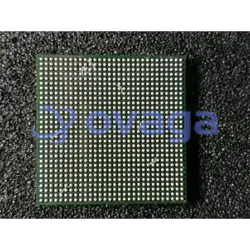
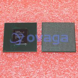
The XC7A35T-2FGG484I chip is a Field-Programmable Gate Array (FPGA) manufactured by Xilinx. It belongs to the Artix-7 family and comes in a 484-ball Fine-Pitch Ball Grid Array (FBGA) package. This chip offers numerous user-programmable logic cells, memory blocks, and I/O pins, making it suitable for various applications requiring programmable logic functionality.
-
Equivalent
Some equivalent products of the XC7A35T-2FGG484I chip include the XC7A35T-1FGG484I and XC7A35T-3FGG484I chips. These alternatives have slightly different specifications, such as lower or higher operating frequency ranges, but offer similar functionality. -
Features
The XC7A35T-2FGG484I is a field-programmable gate array (FPGA) with notable features including 33,280 logic cells, 1,800 Kbits of block RAM, 4,860 slices, 90 DSP slices, and a maximum of 450 MHz clock speed. It offers low power consumption, advanced digital signal processing capabilities, and flexible I/O options for a wide range of applications. -
Pinout
The XC7A35T-2FGG484I is a field-programmable gate array (FPGA) with a pin count of 484. It belongs to the Xilinx Artix-7 family and has a speed grade of -2. The specific pin functions can be found in the datasheet provided by the manufacturer. -
Manufacturer
The manufacturer of the XC7A35T-2FGG484I is Xilinx, Inc. Xilinx is a technology company that specializes in the development and manufacture of programmable logic devices (PLDs) and semiconductor products. They are known for their field-programmable gate arrays (FPGAs) and contribute to a wide range of industries, including automotive, telecommunications, and aerospace. -
Application Field
The XC7A35T-2FGG484I is a field-programmable gate array (FPGA) with a wide range of application areas. It can be used in industries such as automotive, telecommunications, medical devices, aerospace, and defense. With its high logic capacity, low power consumption, and fast performance, this FPGA can handle various complex tasks and computations efficiently. -
Package
The XC7A35T-2FGG484I chip is in a FBGA (Fine-Pitch Ball Grid Array) package type. It has a form factor of 484 pins and its size is 23 x 23 mm.
Datasheet PDF
We provide high quality products, thoughtful service and after sale guarantee
-

We have rich products, can meet your various needs.
-

Minimum order quantity starts from 1pcs.
-

Lowest international shipping fee starts from $0.00
-

365 days quality guarantee for all products