Images are for reference only See Product Specifications
Orders Over
$5000Xilinx XC5VLX30-1FFG676I
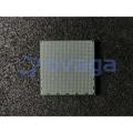
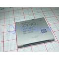
Virtex®-5 LX Field Programmable Gate Array (FPGA) IC 400 1179648 30720 676-BBGA, FCBGA


Brands: AMD Xilinx, Inc
Mfr.Part #: XC5VLX30-1FFG676I
Datasheet: XC5VLX30-1FFG676I Datasheet (PDF)
Package/Case: BGA-676
Product Type: FPGAs (Field Programmable Gate Array)
RoHS Status:
Stock Condition: 3,618 pcs, New Original
Warranty: 1 Year Ovaga Warranty - Find Out More
0
1
XC5VLX30-1FFG676I General Description
Virtex®-5 LX Field Programmable Gate Array (FPGA) IC 400 1179648 30720 676-BBGA, FCBGA
Features
- 33,088 logic cells
- 640 Kb block RAM
- 12 Digital Clock Managers (DCMs)
- 8 Phase-Locked Loops (PLLs)
- 400 MHz maximum operating frequency
- 1.2V core voltage
- 1.5V/2.5V/3.3V auxiliary voltage options
- 676-pin Fine-pitch Ball Grid Array (FBGA) package

Specifications
| Parameter | Value | Parameter | Value |
|---|---|---|---|
| Case/Package | FCBGA | Mount | Surface Mount |
| Number of Pins | 676 | Max Operating Temperature | 100 °C |
| Min Operating Temperature | -40 °C | Number of I/Os | 400 |
| Number of Logic Blocks (LABs) | 2400 | Number of Logic Elements/Cells | 30720 |
| Operating Supply Voltage | 1 V | RAM Size | 144 kB |
| Speed Grade | 1 |
Shipping
| Shipping Type | Ship Fee | Lead Time | |
|---|---|---|---|
 |
DHL | $20.00-$40.00 (0.50 KG) | 2-5 days |
 |
Fedex | $20.00-$40.00 (0.50 KG) | 2-5 days |
 |
UPS | $20.00-$40.00 (0.50 KG) | 2-5 days |
 |
TNT | $20.00-$40.00 (0.50 KG) | 2-5 days |
 |
EMS | $20.00-$40.00 (0.50 KG) | 2-5 days |
 |
REGISTERED AIR MAIL | $20.00-$40.00 (0.50 KG) | 2-5 days |
Processing Time:Shipping fee depend on different zone and country.
Payment
| Terms of payment | Hand Fee | |
|---|---|---|
 |
Wire Transfer | charge US$30.00 banking fee. |
 |
Paypal | charge 4.0% service fee. |
 |
Credit Card | charge 3.5% service fee. |
 |
Western Union | charge US.00 banking fee. |
 |
Money Gram | charge US$0.00 banking fee. |
Guarantees
1.The electronic components you purchase include 365 Days Warranty, We guarantee product quality.
2.If some of the items you received aren't of perfect quality, we would resiponsibly arrange your refund or replacement. But the items must remain their orginal condition.
Packing
-

Step1 :Product
-

Step2 :Vacuum packaging
-

Step3 :Anti-static bag
-

Step4 :Individual packaging
-

Step5 :Packaging boxes
-

Step6 :bar-code shipping tag


All the products will packing in anti-staticbag. Ship with ESD antistatic protection.
Outside ESD packing’s lable will use ourcompany’s information: Part Mumber, Brand and Quantity.
We will inspect all the goods before shipment,ensure all the products at good condition and ensure the parts are new originalmatch datasheet.
After all the goods are ensure no problems afterpacking, we will packing safely and send by global express. It exhibitsexcellent puncture and tear resistance along with good seal integrity.


Part points
-
The XC5VLX30-1FFG676I chip is a field-programmable gate array (FPGA) by Xilinx. It is a reliable and versatile semiconductor component used in various applications like aerospace, automotive, communication, and industrial systems. This chip offers advanced features such as high-performance logic, versatile I/O capabilities, and easy reprogrammability, making it suitable for a wide range of complex designs.
-
Equivalent
The equivalent products of the XC5VLX30-1FFG676I chip are the XC5VFX30-1FFG676I and the XC5VLX30T-1FFG676I programmable logic devices. -
Features
The XC5VLX30-1FFG676I is a field-programmable gate array (FPGA) with 30,816 logic cells, 1,352,500 distributed RAM bits, and a maximum of 1,060 MHz clock speed. It has an on-chip power monitor and built-in cryptographic functionality. The device features adequate internal memory, high logic density, and advanced power management capabilities. -
Pinout
The XC5VLX30-1FFG676I is a FPGA device with 676 pins. It belongs to the Virtex-5 LX family and has a speed grade of -1. The specific function and pin assignment for each pin can be found in the device datasheet provided by Xilinx. -
Manufacturer
The manufacturer of the XC5VLX30-1FFG676I is Xilinx Inc. Xilinx is a technology company that specializes in the development and manufacturing of programmable logic devices (PLDs) and associated technologies. They are known for their field-programmable gate arrays (FPGAs), which are widely used in various applications including telecommunications, automotive, aerospace, and industrial sectors. -
Application Field
The XC5VLX30-1FFG676I is a field-programmable gate array (FPGA) that can be used in various applications such as wireless communication systems, video processing, medical imaging, industrial control systems, and automotive electronics. -
Package
The XC5VLX30-1FFG676I chip is a flip-chip ball grid array (FC-BGA) package. It has a form factor of 676 balls with a grid array of 1 mm pitch. The package size measures approximately 27 x 27 mm.


Datasheet PDF
We provide high quality products, thoughtful service and after sale guarantee
-

We have rich products, can meet your various needs.
-

Minimum order quantity starts from 1pcs.
-

Lowest international shipping fee starts from $0.00
-

365 days quality guarantee for all products