Images are for reference only See Product Specifications
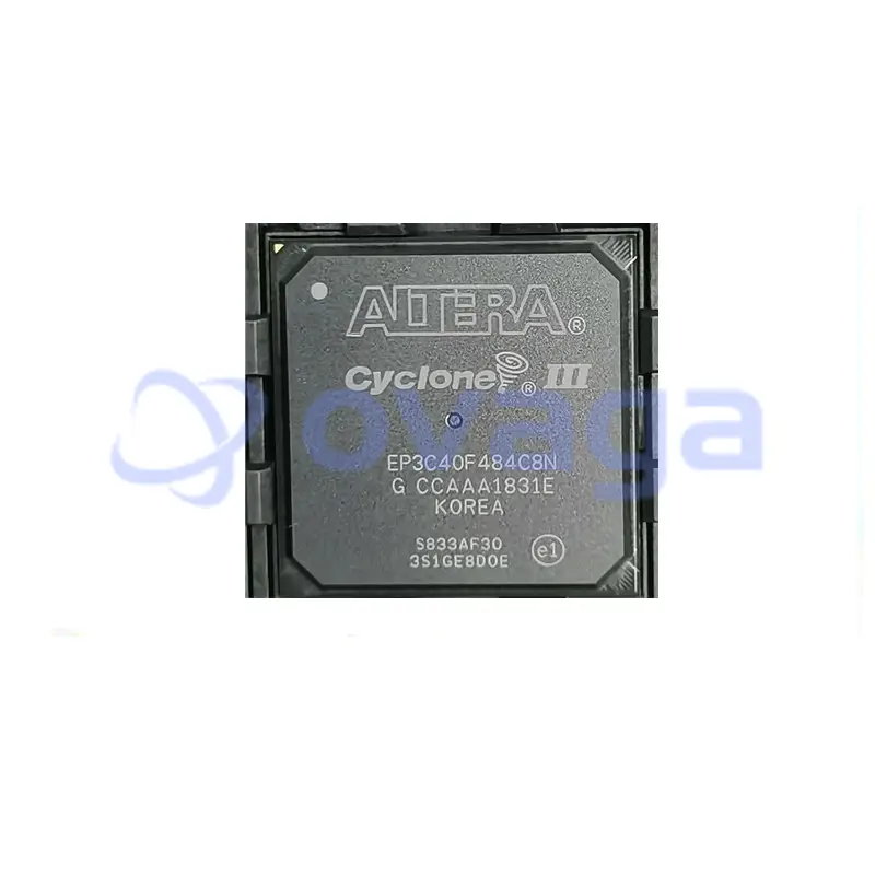
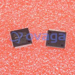
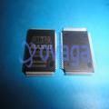
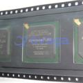
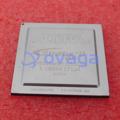
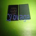
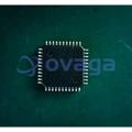
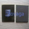
Altera EP3C40F484C8N
Field Programmable Gate Array, 39600 CLBs, 472.5MHz, 39600-Cell, CMOS, PBGA484


Brands: Altera Corporation (Intel)
Mfr.Part #: EP3C40F484C8N
Datasheet: EP3C40F484C8N Datasheet (PDF)
Package/Case: FBGA-484
Product Type: Programmable Logic ICs
RoHS Status:
Stock Condition: 2061 pcs, New Original
Warranty: 1 Year Ovaga Warranty - Find Out More
0
1
Add To BomEP3C40F484C8N General Description
; Logic Type:EP3C40; Logic Base Number:3; No. of I/O Pins:331; Termination Type:SMD; Package/Case:484-FBGA; No. of Pins:484; IC Generic Number:; Operating Temp. Max:85°C; Operating Temp. Min:0°C ;RoHS Compliant: Yes
Features
- It contains 39,600 logic elements (LEs) and 1,260 embedded memory blocks (MBs).
- It has a maximum of 550 user I/O pins.
- It operates at a maximum frequency of 400 MHz.
- It has various configurable features such as PLLs (Phase-Locked Loops), memory controllers, and transceivers.
Application
- Industrial automation
- Video and image processing
- Network processing
- Medical equipment
- Aerospace and defense systems
- Automotive systems
Specifications
| Parameter | Value | Parameter | Value |
|---|---|---|---|
| feature-family-name | Cyclone® III | feature-process-technology | 65nm |
| feature-maximum-number-of-user-i-os | 331 | feature-number-of-registers | |
| feature-device-logic-cells | 39600 | feature-device-system-gates | |
| feature-number-of-multipliers | 126 (18x18) | feature-program-memory-type | SRAM |
| feature-ram-bits-kbit | 1134 | feature-total-number-of-block-ram | 126 |
| feature-ethernet-macs | feature-supported-ip-core | Viterbi Compiler, Low-Speed/Hybrid Serial Decoder|V1 ColdFire|SpeedView Enabled JPEG Encoder (SVE-JPEG-E)|10 Gigabit Ethernet MAC|32/64-bit PCI-X bus Master/Target interface Core, 66/100/133Mhz | |
| feature-supported-ip-core-manufacture | Altera/Freescale/CAST, Inc/MorethanIP/PLDA | feature-maximum-number-of-serdes-channels | |
| feature-device-logic-units | 39600 | feature-device-number-of-dlls-plls | 4 |
| feature-transceiver-blocks | feature-transceiver-speed-gbps | ||
| feature-dedicated-dsp | feature-pci-blocks | ||
| feature-programmability | No | feature-maximum-internal-frequency-mhz | 402 |
| feature-speed-grade | 8 | feature-giga-multiply-accumulates-per-second | |
| feature-differential-i-o-standards-supported | LVPECL|LVDS|HSTL-18|HSTL-15|HSTL-12|SSTL-2|SSTL-18|RSDS | feature-single-ended-i-o-standards-supported | LVTTL|LVCMOS|PCI|PCI-X|SSTL|HSTL |
| feature-external-memory-interface | DDR2 SDRAM|QDRII+SRAM | feature-minimum-operating-supply-voltage-v | 1.15 |
| feature-maximum-operating-supply-voltage-v | 1.25 | feature-packaging | Tray |
| feature-rohs | feature-rad-hard | ||
| feature-pin-count | 484 | feature-supplier-package | FBGA |
| feature-standard-package-name1 | BGA | feature-cecc-qualified | No |
| feature-esd-protection | feature-escc-qualified | ||
| feature-military | No | feature-aec-qualified | No |
| feature-aec-qualified-number | feature-auto-motive | No | |
| feature-p-pap | No | feature-eccn-code | 3A991 |
| feature-svhc | No |
Shipping
| Shipping Type | Ship Fee | Lead Time | |
|---|---|---|---|
 |
DHL | $20.00-$40.00 (0.50 KG) | 2-5 days |
 |
Fedex | $20.00-$40.00 (0.50 KG) | 2-5 days |
 |
UPS | $20.00-$40.00 (0.50 KG) | 2-5 days |
 |
TNT | $20.00-$40.00 (0.50 KG) | 2-5 days |
 |
EMS | $20.00-$40.00 (0.50 KG) | 2-5 days |
 |
REGISTERED AIR MAIL | $20.00-$40.00 (0.50 KG) | 2-5 days |
Processing Time:Shipping fee depend on different zone and country.
Payment
| Terms of payment | Hand Fee | |
|---|---|---|
 |
Wire Transfer | charge US$30.00 banking fee. |
 |
Paypal | charge 4.0% service fee. |
 |
Credit Card | charge 3.5% service fee. |
 |
Western Union | charge US.00 banking fee. |
 |
Money Gram | charge US$0.00 banking fee. |
Guarantees
1.The electronic components you purchase include 365 Days Warranty, We guarantee product quality.
2.If some of the items you received aren't of perfect quality, we would resiponsibly arrange your refund or replacement. But the items must remain their orginal condition.
Packing
-

Step1 :Product
-

Step2 :Vacuum packaging
-

Step3 :Anti-static bag
-

Step4 :Individual packaging
-

Step5 :Packaging boxes
-

Step6 :bar-code shipping tag


All the products will packing in anti-staticbag. Ship with ESD antistatic protection.
Outside ESD packing’s lable will use ourcompany’s information: Part Mumber, Brand and Quantity.
We will inspect all the goods before shipment,ensure all the products at good condition and ensure the parts are new originalmatch datasheet.
After all the goods are ensure no problems afterpacking, we will packing safely and send by global express. It exhibitsexcellent puncture and tear resistance along with good seal integrity.


Equivalent Parts
For the EP3C40F484C8N component, you may consider these replacement and alternative parts:
Part Number
Brands
Package
Description
Part points
-
EP3C40F484C8N is a programmable chip developed by Altera. It belongs to the Cyclone III FPGA family and is designed for a broad range of applications. With 40,000 logic elements, 583 I/O pins, and various high-speed interfaces, it offers high performance and flexibility. The C8N package refers to the chip's 484-pin FineLine BGA package. Overall, EP3C40F484C8N is ideal for complex digital systems and offers customization options through its programmable logic.
-
Equivalent
Equivalent products of the EP3C40F484C8N chip include EP3C40F484I8N, EP3C40F484I7N, EP3C40F484I8LN, and EP3C40F484I7LN from the same Cyclone III FPGA family by Altera/Intel. -
Features
EP3C40F484C8N is a Cyclone III FPGA (Field-Programmable Gate Array) with 40,020 logic elements, 1,134 Kbits RAM, and 346 multiplexers. It operates at a maximum clock frequency of 408 MHz and has 249 user I/O pins. This FPGA offers high performance, low power consumption, and is suited for a wide range of applications. -
Pinout
The EP3C40F484C8N is an FPGA with a pin count of 484. Its function is to program and configure digital logic circuits to perform specific tasks. The FPGA can be customized to meet specific requirements and is often used in applications such as telecommunications, image and video processing, and embedded systems. -
Manufacturer
EP3C40F484C8N is manufactured by Altera, which is a company specializing in the production of programmable logic devices and associated software and development tools. Altera, now a part of Intel Corporation, offers a range of FPGA (field-programmable gate array) solutions for various applications in sectors like automotive, telecommunications, industrial automation, and more. -
Application Field
The EP3C40F484C8N is a field-programmable gate array (FPGA) that is commonly used in various applications such as automotive systems, industrial automation, communication systems, and image and video processing. Its high-performance and flexible architecture make it suitable for a wide range of electronic design projects. -
Package
The EP3C40F484C8N chip is offered in a standard plastic package of FBGA (Fine-pitch Ball Grid Array) type. It has 484 contacts and its form, or physical dimensions, are designed for a small footprint, making it suitable for various applications.
Datasheet PDF
We provide high quality products, thoughtful service and after sale guarantee
-

We have rich products, can meet your various needs.
-

Minimum order quantity starts from 1pcs.
-

Lowest international shipping fee starts from $0.00
-

365 days quality guarantee for all products