Images are for reference only See Product Specifications
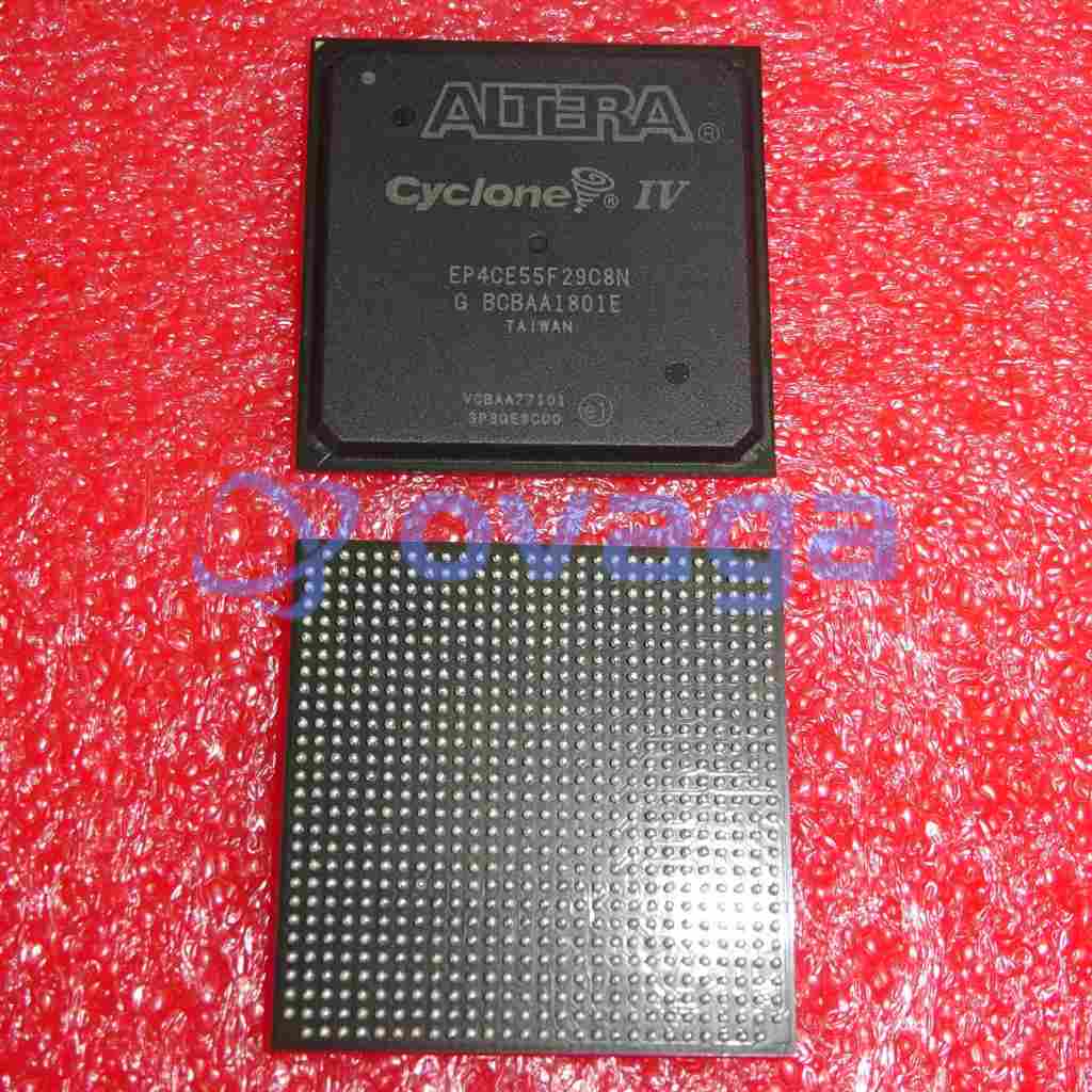
Altera EP3C25F324C8
FPGA Cyclone® III Family 24624 Cells 402MHz 65nm Technology 1.2V 324-Pin FBGA


Brands: Altera Corporation (Intel)
Mfr.Part #: EP3C25F324C8
Datasheet: EP3C25F324C8 Datasheet (PDF)
Package/Case: FBGA-324
RoHS Status:
Stock Condition: 3079 pcs, New Original
Product Type: Programmable Logic ICs
0
1
*All prices are in USD
| Qty | Unit Price | Ext Price |
|---|---|---|
| 1 | $105.357 | $105.357 |
| 200 | $40.774 | $8154.800 |
| 500 | $39.339 | $19669.500 |
| 1000 | $38.632 | $38632.000 |
In Stock:3079 PCS
EP3C25F324C8 General Description
Cyclone® III Field Programmable Gate Array (FPGA) IC 215 608256 24624 324-BGA
Features
- Logic Elements: 24,624
- RAM: 518,144 bits
- Multipliers: 48
- PLLs: 4
- Maximum user I/O pins: 208
Application
- Industrial automation
- Test and measurement
- Video and image processing
- Communication equipment
- Medical imaging
- Military and aerospace
 Inventory")
Specifications
| Parameter | Value | Parameter | Value |
|---|---|---|---|
| feature-family-name | Cyclone® III | feature-process-technology | 65nm |
| feature-maximum-number-of-user-i-os | 215 | feature-number-of-registers | |
| feature-device-logic-cells | 24624 | feature-device-system-gates | |
| feature-number-of-multipliers | 66 (18x18) | feature-program-memory-type | SRAM |
| feature-ram-bits-kbit | 594 | feature-total-number-of-block-ram | 66 |
| feature-ethernet-macs | feature-supported-ip-core | SpeedView Enabled JPEG Encoder (SVE-JPEG-E)|V1 ColdFire|Viterbi Compiler, Low-Speed/Hybrid Serial Decoder|32/64-bit PCI-X bus Master/Target interface Core, 66/100/133Mhz|10 Gigabit Ethernet MAC | |
| feature-supported-ip-core-manufacture | Altera/Freescale/CAST, Inc/MorethanIP/PLDA | feature-maximum-number-of-serdes-channels | |
| feature-device-logic-units | 24624 | feature-device-number-of-dlls-plls | 4 |
| feature-transceiver-blocks | feature-transceiver-speed-gbps | ||
| feature-dedicated-dsp | feature-pci-blocks | ||
| feature-programmability | No | feature-maximum-internal-frequency-mhz | 402 |
| feature-speed-grade | 8 | feature-giga-multiply-accumulates-per-second | |
| feature-differential-i-o-standards-supported | RSDS|SSTL-18|SSTL-2|HSTL-12|HSTL-15|HSTL-18|LVDS|LVPECL | feature-single-ended-i-o-standards-supported | HSTL|SSTL|PCI-X|PCI|LVCMOS|LVTTL |
| feature-external-memory-interface | QDRII+SRAM|DDR2 SDRAM | feature-minimum-operating-supply-voltage-v | 1.15 |
| feature-maximum-operating-supply-voltage-v | 1.25 | feature-packaging | |
| feature-rohs | feature-rad-hard | ||
| feature-pin-count | 324 | feature-supplier-package | FBGA |
| feature-standard-package-name1 | BGA | feature-cecc-qualified | No |
| feature-esd-protection | feature-escc-qualified | ||
| feature-military | No | feature-aec-qualified | No |
| feature-aec-qualified-number | feature-auto-motive | No | |
| feature-p-pap | No | feature-eccn-code | 3A991 |
| feature-svhc | Yes |
Shipping
| Shipping Type | Ship Fee | Lead Time | |
|---|---|---|---|
 |
DHL | $20.00-$40.00 (0.50 KG) | 2-5 days |
 |
Fedex | $20.00-$40.00 (0.50 KG) | 2-5 days |
 |
UPS | $20.00-$40.00 (0.50 KG) | 2-5 days |
 |
TNT | $20.00-$40.00 (0.50 KG) | 2-5 days |
 |
EMS | $20.00-$40.00 (0.50 KG) | 2-5 days |
 |
REGISTERED AIR MAIL | $20.00-$40.00 (0.50 KG) | 2-5 days |
Processing Time:Shipping fee depend on different zone and country.
Payment
| Terms of payment | Hand Fee | |
|---|---|---|
 |
Wire Transfer | charge US$30.00 banking fee. |
 |
Paypal | charge 4.0% service fee. |
 |
Credit Card | charge 3.5% service fee. |
 |
Western Union | charge US.00 banking fee. |
 |
Money Gram | charge US$0.00 banking fee. |
Guarantees
1.The electronic components you purchase include 365 Days Warranty, We guarantee product quality.
2.If some of the items you received aren't of perfect quality, we would resiponsibly arrange your refund or replacement. But the items must remain their orginal condition.
Packing
-

Step1 :Product
-

Step2 :Vacuum packaging
-

Step3 :Anti-static bag
-

Step4 :Individual packaging
-

Step5 :Packaging boxes
-

Step6 :bar-code shipping tag
All the products will packing in anti-staticbag. Ship with ESD antistatic protection.
Outside ESD packing’s lable will use ourcompany’s information: Part Mumber, Brand and Quantity.
We will inspect all the goods before shipment,ensure all the products at good condition and ensure the parts are new originalmatch datasheet.
After all the goods are ensure no problems afterpacking, we will packing safely and send by global express. It exhibitsexcellent puncture and tear resistance along with good seal integrity.


Equivalent Parts
For the EP3C25F324C8 component, you may consider these replacement and alternative parts:
Part Number
Brands
Package
Description
Part Number : XC6SLX25-2FTG256C
Brands :
Package :
Description : XC6SLX25-2FTG256C
Part points
-
The EP3C25F324C8 is a low-cost, low-power FPGA chip from Intel (formerly Altera) that offers a balance of resources, performance, and power consumption for a wide range of applications. With 25,000 logic elements, 324 Kbits of embedded memory, and various I/O interfaces, it is suitable for designs requiring moderate complexity and flexibility.
-
Equivalent
Some equivalent products of EP3C25F324C8 chip are Altera Cyclone III FPGA EP3C25F324C6, Altera Cyclone III FPGA EP3C25F324I7, and Altera Cyclone III FPGA EP3C25F324C6N. These chips offer similar features and performance characteristics to the EP3C25F324C8 chip. -
Features
1. 25,000 logic elements 2. 324 Kbits of RAM 3. 8 embedded Multiplier blocks 4. Low power consumption 5. Maximum internal clock frequency of 450 MHz 6. Built-in PLLs for clock management 7. Comprehensive set of I/O standards 8. Easy to program and configure through Quartus II software. -
Pinout
The EP3C25F324C8 is a FPGA with 324 pins. It is a low-cost, low-power device with a capacity of 25,000 logic elements (LEs), suitable for a wide range of applications such as industrial, automotive, and communication systems. The pins are used for IO, configuration, and power supply. -
Manufacturer
The EP3C25F324C8 is manufactured by Altera Corporation, now a part of Intel Corporation. Altera specialized in designing and manufacturing programmable logic devices (PLDs), particularly field-programmable gate arrays (FPGAs). These components are widely used in various industries for their flexibility and reconfigurability in electronic systems. -
Application Field
The EP3C25F324C8 is a field-programmable gate array (FPGA) commonly used in industrial automation, communications, medical devices, and consumer electronics applications. It is suitable for tasks such as signal processing, data encryption, network communication, and general-purpose computing due to its versatile and configurable nature. -
Package
The EP3C25F324C8 chip is packaged in a plastic ball grid array (PBGA) with 324 pins. It comes in a 17mm x 17mm form factor and has a size of 324-ball FBGA (15x15 mm, 1.0 mm pitch).
Datasheet PDF
We provide high quality products, thoughtful service and after sale guarantee
-

We have rich products, can meet your various needs.
-

Minimum order quantity starts from 1pcs.
-

Lowest international shipping fee starts from $0.00
-

365 days quality guarantee for all products