

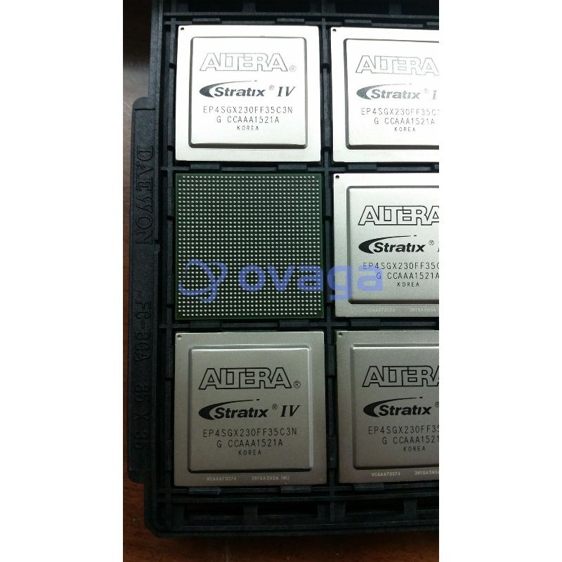
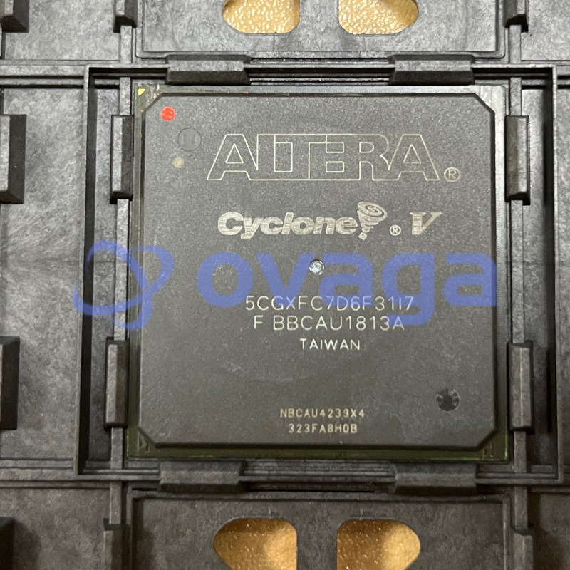
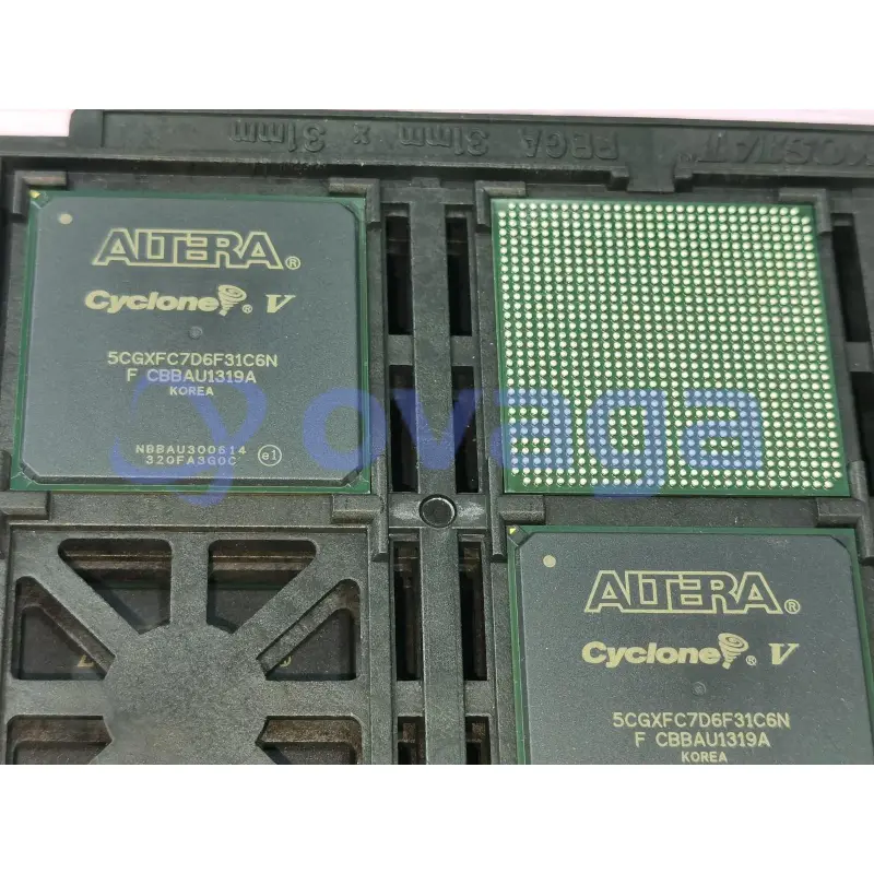
Images are for reference only See Product Specifications
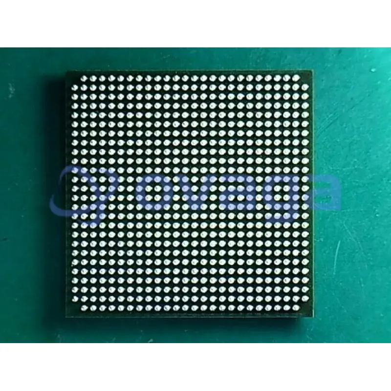
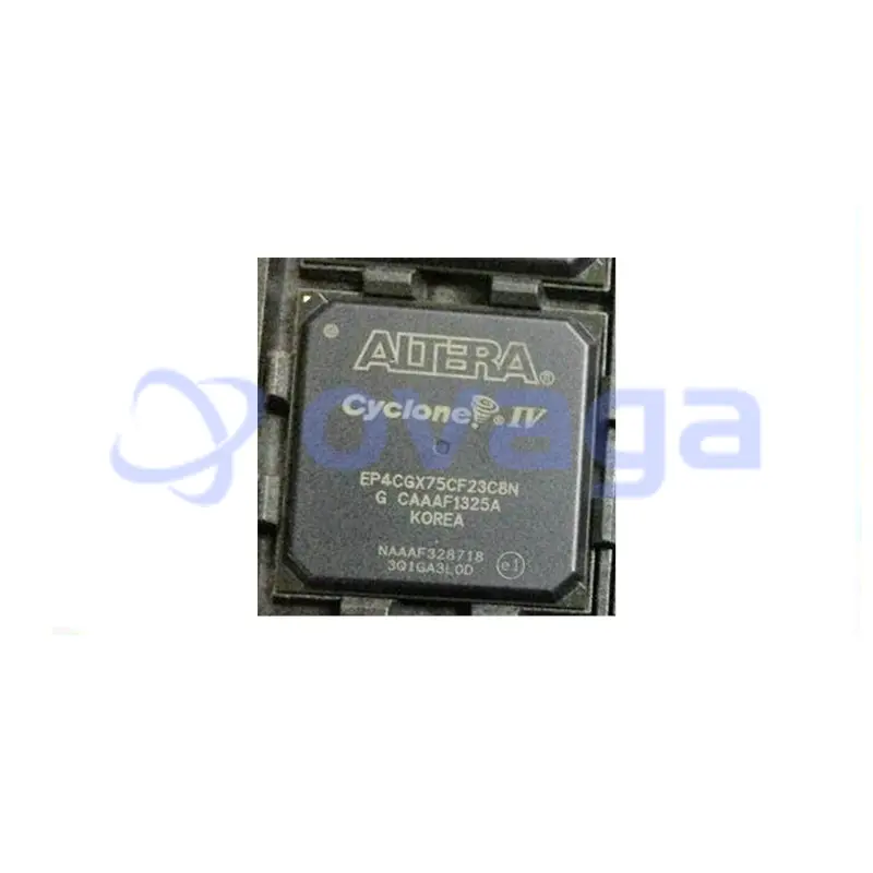
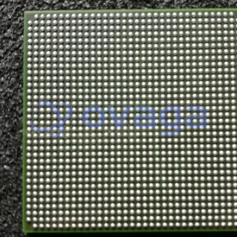
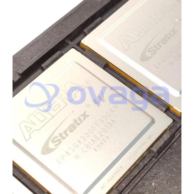
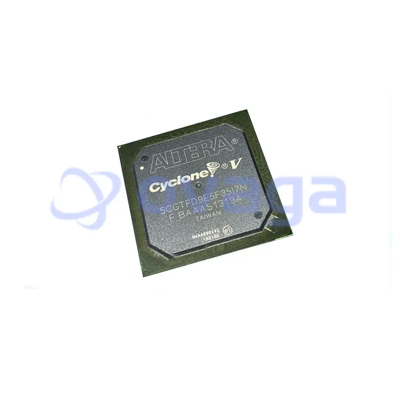
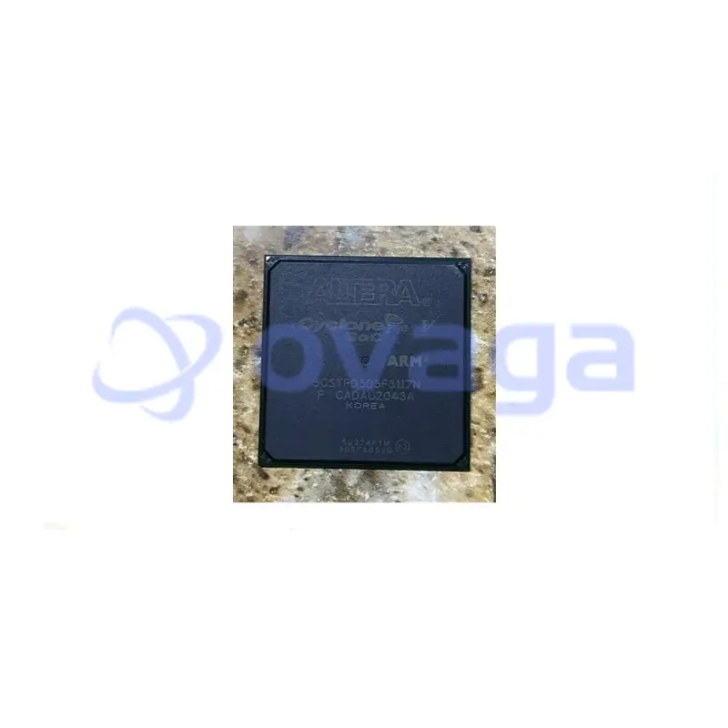
Altera 5CGTFD5C5F27C7N
FPGA Cyclone® V GT Family 77000 Cells 28nm Technology 1.1V 672-Pin FBGA


Brands: Altera Corporation (Intel)
Mfr.Part #: 5CGTFD5C5F27C7N
Datasheet: 5CGTFD5C5F27C7N Datasheet (PDF)
Package/Case: FBGA-672
Product Type: Programmable Logic ICs
5CGTFD5C5F27C7N General Description
Cyclone® V GT Field Programmable Gate Array (FPGA) IC 336 5001216 77000 672-BGA
 Inventory")
Specifications
| Parameter | Value | Parameter | Value |
|---|---|---|---|
| feature-family-name | Cyclone® V GT | feature-process-technology | 28nm |
| feature-maximum-number-of-user-i-os | 336 | feature-number-of-registers | 116320 |
| feature-device-logic-cells | 77000 | feature-device-system-gates | |
| feature-number-of-multipliers | 300 (18x18) | feature-program-memory-type | SRAM |
| feature-ram-bits-kbit | 4460 | feature-total-number-of-block-ram | 446 |
| feature-ethernet-macs | 2 | feature-supported-ip-core | |
| feature-supported-ip-core-manufacture | feature-maximum-number-of-serdes-channels | ||
| feature-device-logic-units | 77000 | feature-device-number-of-dlls-plls | 6 |
| feature-transceiver-blocks | 6 | feature-transceiver-speed-gbps | 6.144 |
| feature-dedicated-dsp | 150 | feature-pci-blocks | 2 |
| feature-programmability | Yes | feature-maximum-internal-frequency-mhz | |
| feature-speed-grade | 7 | feature-giga-multiply-accumulates-per-second | |
| feature-differential-i-o-standards-supported | LVPECL|LVDS | feature-single-ended-i-o-standards-supported | LVTTL|LVCMOS |
| feature-external-memory-interface | DDR2 SDRAM|DDR3 SDRAM|LPDDR2 | feature-minimum-operating-supply-voltage-v | 1.07 |
| feature-maximum-operating-supply-voltage-v | 1.13 | feature-packaging | |
| feature-rohs | feature-rad-hard | ||
| feature-pin-count | 672 | feature-supplier-package | FBGA |
| feature-standard-package-name1 | BGA | feature-cecc-qualified | No |
| feature-esd-protection | feature-escc-qualified | ||
| feature-military | No | feature-aec-qualified | No |
| feature-aec-qualified-number | feature-auto-motive | No | |
| feature-p-pap | No | feature-eccn-code | 3A991 |
| feature-svhc | No |
Shipping
| Shipping Type | Ship Fee | Lead Time | |
|---|---|---|---|
 |
DHL | $20.00-$40.00 (0.50 KG) | 2-5 days |
 |
Fedex | $20.00-$40.00 (0.50 KG) | 2-5 days |
 |
UPS | $20.00-$40.00 (0.50 KG) | 2-5 days |
 |
TNT | $20.00-$40.00 (0.50 KG) | 2-5 days |
 |
EMS | $20.00-$40.00 (0.50 KG) | 2-5 days |
 |
REGISTERED AIR MAIL | $20.00-$40.00 (0.50 KG) | 2-5 days |
Processing Time:Shipping fee depend on different zone and country.
Payment
| Terms of payment | Hand Fee | |
|---|---|---|
 |
Wire Transfer | charge US$30.00 banking fee. |
 |
Paypal | charge 4.0% service fee. |
 |
Credit Card | charge 3.5% service fee. |
 |
Western Union | charge US.00 banking fee. |
 |
Money Gram | charge US$0.00 banking fee. |
Guarantees
1.The electronic components you purchase include 365 Days Warranty, We guarantee product quality.
2.If some of the items you received aren't of perfect quality, we would resiponsibly arrange your refund or replacement. But the items must remain their orginal condition.
Packing
-

Step1 :Product
-

Step2 :Vacuum packaging
-

Step3 :Anti-static bag
-

Step4 :Individual packaging
-

Step5 :Packaging boxes
-

Step6 :bar-code shipping tag
All the products will packing in anti-staticbag. Ship with ESD antistatic protection.
Outside ESD packing’s lable will use ourcompany’s information: Part Mumber, Brand and Quantity.
We will inspect all the goods before shipment,ensure all the products at good condition and ensure the parts are new originalmatch datasheet.
After all the goods are ensure no problems afterpacking, we will packing safely and send by global express. It exhibitsexcellent puncture and tear resistance along with good seal integrity.


Part points
-
The 5CGTFD5C5F27C7N chip is a field-programmable gate array (FPGA) developed by Intel (formerly Altera). It belongs to the Stratix V family and offers advanced programmability, high-performance computing capabilities, and versatility for various applications. It features high-speed serial transceivers, embedded memory blocks, digital signal processing capabilities, and is commonly used in fields such as aerospace, telecommunications, and high-performance computing.
-
Features
5CGTFD5C5F27C7N is a Field-Programmable Gate Array (FPGA) from Intel. Its features include a capacity of 270,000 logic elements, 19.7 Mb of embedded memory, built-in transceivers with up to 12.5 Gbps data rates, and support for various communication protocols. The FPGA is designed to offer high performance and flexibility for a wide range of applications. -
Pinout
The 5CGTFD5C5F27C7N is an FPGA (Field-Programmable Gate Array) device manufactured by Intel (previously Altera). It has a pin count of 780, which includes various I/O (input/output) pins for communication with external devices and power supply connections. The specific function of this device will depend on the user's programming and application requirements. -
Manufacturer
Intel Corporation is the manufacturer of the 5CGTFD5C5F27C7N. It is an American multinational corporation that specializes in the design and production of semiconductor chips and related technology. -
Application Field
The 5CGTFD5C5F27C7N FPGA can be used in a wide range of application areas, including telecommunications, networking, data centers, industrial automation, and military technology. Its versatility makes it suitable for various high-performance computing and efficient processing tasks. -
Package
The 5CGTFD5C5F27C7N chip is available in a FBGA (Fine-pitch Ball Grid Array) package type. It has a specific form factor that follows the 27x27 mm size.
Datasheet PDF
We provide high quality products, thoughtful service and after sale guarantee
-

We have rich products, can meet your various needs.
-

Minimum order quantity starts from 1pcs.
-

Lowest international shipping fee starts from $0.00
-

365 days quality guarantee for all products
These components were perfect for my project. Thanks to Ovaga for providing top-notched products and service.