Images are for reference only See Product Specifications
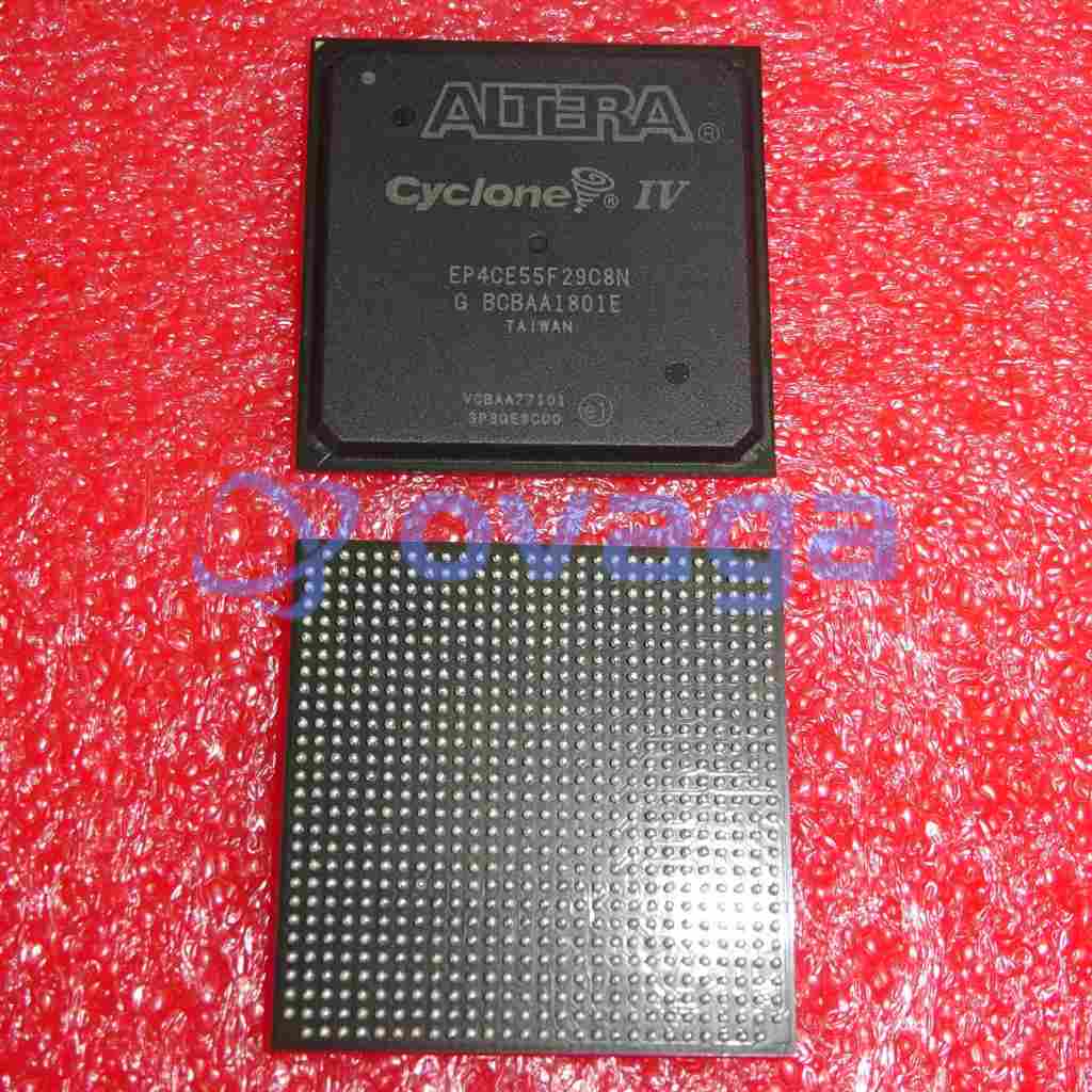
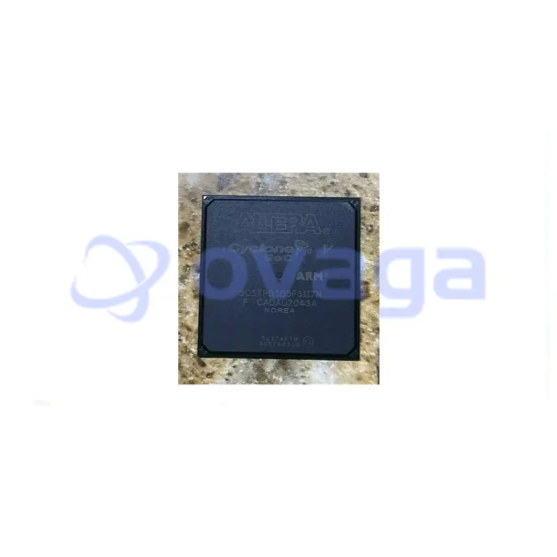
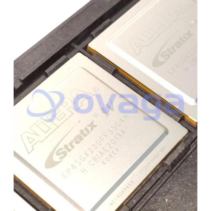
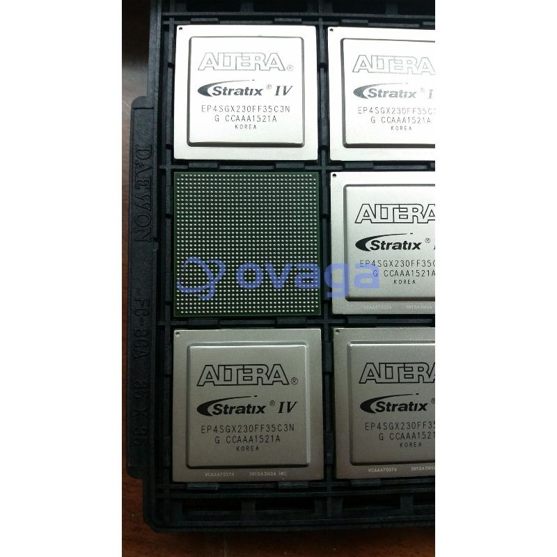
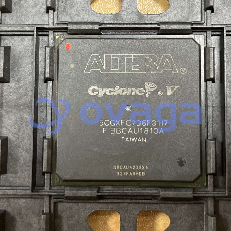
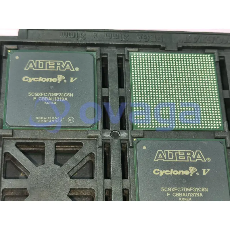
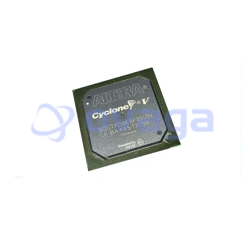
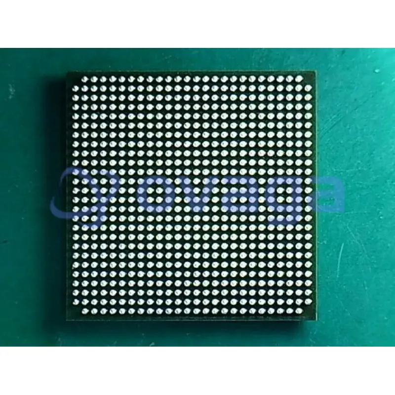
Altera 5CSTFD5D5F31I7N
Dual ARM® Cortex®-A9 MPCore™ with CoreSight™ System On Chip (SOC) IC Cyclone® V ST FPGA - 85K Logic Elements 800MHz 896-FBGA (31x31)


Brands: Altera Corporation (Intel)
Mfr.Part #: 5CSTFD5D5F31I7N
Datasheet: 5CSTFD5D5F31I7N Datasheet (PDF)
Package/Case: UBGA-672
Product Type: Programmable Logic ICs
5CSTFD5D5F31I7N General Description
Dual ARM® Cortex®-A9 MPCore™ with CoreSight™ System On Chip (SOC) IC Cyclone® V ST FPGA - 85K Logic Elements 800MHz 896-FBGA (31x31)
 Inventory")
Specifications
| Parameter | Value | Parameter | Value |
|---|---|---|---|
| Manufacturer: | Intel | Product Category: | SoC FPGA |
| RoHS: | Details | Mounting Style: | SMD/SMT |
| Package / Case: | UBGA-672 | Core: | ARM Cortex A9 |
| Number of Cores: | 2 Core | Maximum Clock Frequency: | 925 MHz |
| L1 Cache Instruction Memory: | 2 x 32 kB | L1 Cache Data Memory: | 2 x 32 kB |
| Program Memory Size: | - | Data RAM Size: | - |
| Number of Logic Elements: | 85000 LE | Adaptive Logic Modules - ALMs: | 32070 ALM |
| Embedded Memory: | 3970 kbit | Number of I/Os: | 288 I/O |
| Operating Supply Voltage: | 1.1 V | Minimum Operating Temperature: | - 40 C |
| Maximum Operating Temperature: | + 100 C | Brand: | Intel / Altera |
| Embedded Block RAM - EBR: | 480 kbit | Maximum Operating Frequency: | 800 MHz |
| Moisture Sensitive: | Yes | Number of Logic Array Blocks - LABs: | 3207 LAB |
| Number of Transceivers: | 9 Transceiver | Packaging: | Tray |
| Product Type: | FPGA - Field Programmable Gate Array | Series: | 5CSTFD5D |
| Factory Pack Quantity: | 27 | Subcategory: | SOC - Systems on a Chip |
| Tradename: | Cyclone | Part # Aliases: | 968388 |
| Unit Weight: | 0.423288 oz |
Shipping
| Shipping Type | Ship Fee | Lead Time | |
|---|---|---|---|
 |
DHL | $20.00-$40.00 (0.50 KG) | 2-5 days |
 |
Fedex | $20.00-$40.00 (0.50 KG) | 2-5 days |
 |
UPS | $20.00-$40.00 (0.50 KG) | 2-5 days |
 |
TNT | $20.00-$40.00 (0.50 KG) | 2-5 days |
 |
EMS | $20.00-$40.00 (0.50 KG) | 2-5 days |
 |
REGISTERED AIR MAIL | $20.00-$40.00 (0.50 KG) | 2-5 days |
Processing Time:Shipping fee depend on different zone and country.
Payment
| Terms of payment | Hand Fee | |
|---|---|---|
 |
Wire Transfer | charge US$30.00 banking fee. |
 |
Paypal | charge 4.0% service fee. |
 |
Credit Card | charge 3.5% service fee. |
 |
Western Union | charge US.00 banking fee. |
 |
Money Gram | charge US$0.00 banking fee. |
Guarantees
1.The electronic components you purchase include 365 Days Warranty, We guarantee product quality.
2.If some of the items you received aren't of perfect quality, we would resiponsibly arrange your refund or replacement. But the items must remain their orginal condition.
Packing
-

Step1 :Product
-

Step2 :Vacuum packaging
-

Step3 :Anti-static bag
-

Step4 :Individual packaging
-

Step5 :Packaging boxes
-

Step6 :bar-code shipping tag
All the products will packing in anti-staticbag. Ship with ESD antistatic protection.
Outside ESD packing’s lable will use ourcompany’s information: Part Mumber, Brand and Quantity.
We will inspect all the goods before shipment,ensure all the products at good condition and ensure the parts are new originalmatch datasheet.
After all the goods are ensure no problems afterpacking, we will packing safely and send by global express. It exhibitsexcellent puncture and tear resistance along with good seal integrity.


Part points
-
The 5CSTFD5D5F31I7N is a high-performance field-programmable gate array (FPGA) chip developed by Intel. This chip offers advanced programmable logic capabilities and high-speed processing for a variety of applications, including networking, data center acceleration, and industrial automation. It features high memory capacity, low power consumption, and enhanced security features, making it an ideal choice for demanding computing tasks.
-
Equivalent
Some equivalent products of the 5CSTFD5D5F31I7N chip are 5CSTFD5D5F31I7N-I, 5CSTFD5D5F31I7N-D, and 5CSTFD5D5F31I7N-X. These chips have similar functionalities and features, but may vary slightly in specifications or performance. -
Features
1. 5CSTFD5D5F31I7N is a high-performance FPGA from Intel. 2. It features a capacity of 114K logic elements and 3,548 Kbits of embedded memory. 3. The FPGA supports 55.3 Mb/s transceiver data rates. 4. It includes dual-core ARM Cortex-A9 processors for embedded processing. 5. The device offers power efficiency and security features for deployment in various applications. -
Pinout
The 5CSTFD5D5F31I7N is a Field-Programmable Gate Array (FPGA) with a pin count of 2176. It is part of the Intel Cyclone V family and features 31,040 logic elements. The functionalities of the pins include I/O, clocks, configuration, power, and ground connections. -
Manufacturer
The manufacturer of the 5CSTFD5D5F31I7N is Intel Corporation. It is an American multinational corporation that produces and sells microprocessors and other computer hardware. Intel is one of the world's largest and highest-valued semiconductor chip makers. -
Application Field
The 5CSTFD5D5F31I7N is used in a wide range of application areas such as automotive, industrial automation, telecommunications, and medical devices. It is ideal for high-performance computing, image processing, signal processing, and artificial intelligence applications that require low power consumption and high processing speeds. -
Package
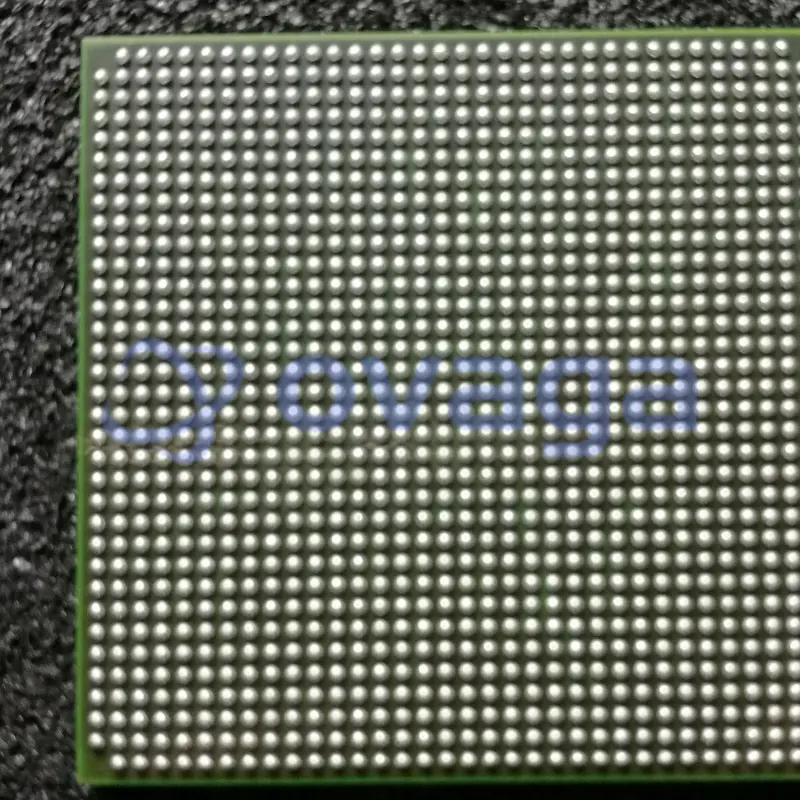
The 5CSTFD5D5F31I7N chip comes in a Ball Grid Array (BGA) package with a 31x31mm form factor.
We provide high quality products, thoughtful service and after sale guarantee
-

We have rich products, can meet your various needs.
-

Minimum order quantity starts from 1pcs.
-

Lowest international shipping fee starts from $0.00
-

365 days quality guarantee for all products