

Images are for reference only See Product Specifications
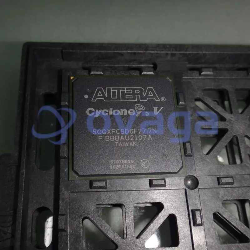
Altera 5CGXFC9D6F27I7N
FPGA Cyclone® V GX Family 301000 Cells 28nm Technology 1.1V 672-Pin FBGA


Brands: Altera Corporation (Intel)
Mfr.Part #: 5CGXFC9D6F27I7N
Datasheet: 5CGXFC9D6F27I7N Datasheet (PDF)
Package/Case: FBGA-672
Product Type: Programmable Logic ICs
RoHS Status:
Stock Condition: 2460 pcs, New Original
Warranty: 1 Year Ovaga Warranty - Find Out More
0
1
Add To Bom5CGXFC9D6F27I7N General Description
Cyclone® V GX Field Programmable Gate Array (FPGA) IC 336 14251008 301000 672-BGA
 Inventory")
Specifications
| Parameter | Value | Parameter | Value |
|---|---|---|---|
| feature-family-name | Cyclone® V GX | feature-process-technology | 28nm |
| feature-maximum-number-of-user-i-os | 336 | feature-number-of-registers | 454240 |
| feature-device-logic-cells | 301000 | feature-device-system-gates | |
| feature-number-of-multipliers | 684 (18x18) | feature-program-memory-type | SRAM |
| feature-ram-bits-kbit | 12200 | feature-total-number-of-block-ram | 1220 |
| feature-ethernet-macs | 2 | feature-supported-ip-core | |
| feature-supported-ip-core-manufacture | feature-maximum-number-of-serdes-channels | ||
| feature-device-logic-units | 301000 | feature-device-number-of-dlls-plls | 8 |
| feature-transceiver-blocks | 12 | feature-transceiver-speed-gbps | 3.125 |
| feature-dedicated-dsp | 342 | feature-pci-blocks | 2 |
| feature-programmability | Yes | feature-maximum-internal-frequency-mhz | |
| feature-speed-grade | 7 | feature-giga-multiply-accumulates-per-second | |
| feature-differential-i-o-standards-supported | LVPECL|LVDS | feature-single-ended-i-o-standards-supported | LVTTL|LVCMOS |
| feature-external-memory-interface | DDR2 SDRAM|DDR3 SDRAM|LPDDR2 | feature-minimum-operating-supply-voltage-v | 1.07 |
| feature-maximum-operating-supply-voltage-v | 1.13 | feature-packaging | |
| feature-rohs | feature-rad-hard | ||
| feature-pin-count | 672 | feature-supplier-package | FBGA |
| feature-standard-package-name1 | BGA | feature-cecc-qualified | No |
| feature-esd-protection | feature-escc-qualified | ||
| feature-military | No | feature-aec-qualified | No |
| feature-aec-qualified-number | feature-auto-motive | No | |
| feature-p-pap | No | feature-eccn-code | 3A991 |
| feature-svhc | No |
Shipping
| Shipping Type | Ship Fee | Lead Time | |
|---|---|---|---|
 |
DHL | $20.00-$40.00 (0.50 KG) | 2-5 days |
 |
Fedex | $20.00-$40.00 (0.50 KG) | 2-5 days |
 |
UPS | $20.00-$40.00 (0.50 KG) | 2-5 days |
 |
TNT | $20.00-$40.00 (0.50 KG) | 2-5 days |
 |
EMS | $20.00-$40.00 (0.50 KG) | 2-5 days |
 |
REGISTERED AIR MAIL | $20.00-$40.00 (0.50 KG) | 2-5 days |
Processing Time:Shipping fee depend on different zone and country.
Payment
| Terms of payment | Hand Fee | |
|---|---|---|
 |
Wire Transfer | charge US$30.00 banking fee. |
 |
Paypal | charge 4.0% service fee. |
 |
Credit Card | charge 3.5% service fee. |
 |
Western Union | charge US.00 banking fee. |
 |
Money Gram | charge US$0.00 banking fee. |
Guarantees
1.The electronic components you purchase include 365 Days Warranty, We guarantee product quality.
2.If some of the items you received aren't of perfect quality, we would resiponsibly arrange your refund or replacement. But the items must remain their orginal condition.
Packing
-

Step1 :Product
-

Step2 :Vacuum packaging
-

Step3 :Anti-static bag
-

Step4 :Individual packaging
-

Step5 :Packaging boxes
-

Step6 :bar-code shipping tag


All the products will packing in anti-staticbag. Ship with ESD antistatic protection.
Outside ESD packing’s lable will use ourcompany’s information: Part Mumber, Brand and Quantity.
We will inspect all the goods before shipment,ensure all the products at good condition and ensure the parts are new originalmatch datasheet.
After all the goods are ensure no problems afterpacking, we will packing safely and send by global express. It exhibitsexcellent puncture and tear resistance along with good seal integrity.


Part points
-
5CGXFC9D6F27I7N is a high-performance field-programmable gate array (FPGA) chip developed by Intel. It features a capacity of 9 million logic elements, making it powerful for various applications. The chip offers high-speed and low-latency performance, along with advanced security features and connectivity interfaces. It can be programmed and reconfigured in the field, enabling flexibility for different hardware designs. Overall, the 5CGXFC9D6F27I7N is a versatile FPGA chip suitable for demanding applications.
-
Features
The 5CGXFC9D6F27I7N is a field-programmable gate array (FPGA) device from Intel. Its notable features include 150,000 logic elements, 634 user I/Os, 9,360 Kbits of embedded memory, 356 18x18 multiply-accumulate (MAC) blocks, and support for various high-speed communication protocols. -
Pinout
The 5CGXFC9D6F27I7N is a Field-Programmable Gate Array (FPGA) from Intel. It has a pin count of 780 and offers various functions including logic functions, memory blocks, high-speed transceivers, and I/O interfaces. -
Manufacturer
Intel is the manufacturer of the 5CGXFC9D6F27I7N. Intel is an American multinational corporation that designs and manufactures integrated digital technology platforms. The company is known for its processors and other computer-related products, and it also provides a wide range of services including cloud computing, data centers, and Internet of Things (IoT) solutions. -
Application Field
The 5CGXFC9D6F27I7N is a field-programmable gate array (FPGA) device manufactured by Intel. It is commonly used in a wide range of applications such as telecommunications, networking, military and aerospace, industrial automation, video and image processing, and high-performance computing. -
Package
The 5CGXFC9D6F27I7N chip is a Field-Programmable Gate Array (FPGA) offered in a Ball Grid Array (BGA) package. It has a form factor of 27x27 mm.


Datasheet PDF
We provide high quality products, thoughtful service and after sale guarantee
-

We have rich products, can meet your various needs.
-

Minimum order quantity starts from 1pcs.
-

Lowest international shipping fee starts from $0.00
-

365 days quality guarantee for all products


We've come to rely on Ovaga for all of our component needs.