Images are for reference only See Product Specifications
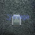
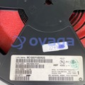
ON MC100EP195FAR2G
Active Programmable Delay Line with 1-IN and 0.01ns Absolute Delay


Brands: Onsemi
Mfr.Part #: MC100EP195FAR2G
Datasheet: MC100EP195FAR2G Datasheet (PDF)
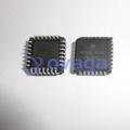
Package/Case: LQFP-32
Product Type: Clock & Timer ICs
RoHS Status:
Stock Condition: 3877 pcs, New Original
Warranty: 1 Year Ovaga Warranty - Find Out More
0
1
Add To BomMC100EP195FAR2G General Description
NECL/PECL input transition.
The delay section consists of a programmable matrix of gates and multiplexers as shown in the data sheet logic diagram. The delay increment of the EP195 has a digitally selectable resolution of about 10 ps and a range of up to 10.2 ns. The required delay is selected by the 10 data select inputs D(0:9) which are latched on chip by a high signal on the latch enable (LEN) control. The MC10/100EP195 is a programmable delay chip (PDC) designed primarily for clock deskewing and timing adjustment. It provides variable delay of a differential The approximate delay values for varying tap numbers correlating to D0 (LSB) through D9 (MSB) are shown in the data sheet.
Because the EP195 is designed using a chain of multiplexers it has a fixed minimum delay of 2.2 ns. An additional pin D10 is provided for cascading multiple PDCs for increased programmable range. The cascade logic allows full control of multiple PDCs.
Select input pins D0-D10 may be threshold controlled by combinations of interconnects between VEF (pin 7) and VCF (pin 8) for CMOS, ECL, or TTL level signals. For CMOS input levels, leave VCF and VEF open. For ECL operation, short VCF and VEF (pins 7 and 8). For TTL level operation, connect a 1.5 V supply reference to VCF and leave open VEF pin. The 1.5 V reference voltage to VCF pin can be accomplished by placing a 1.5k Ohm or 500 Ohm resistor between VCF and VEE for 3.3 V or 5.0 V power supplies, respectively.
The VBB pin, an internally generated voltage supply, is available to this device only. For single-ended input conditions, the unused differential input is connected to VBB as a switching reference voltage. VBB may also rebias AC coupled inputs. When used, decouple VBB and VCC via a 0.01 uF capacitor and limit current sourcing or
Features
- Maximum Frequency > 1.2 Ghz Typical
- Programmable Range: 2.2 ns to 12.2 ns
- 10 ps Increments
- PECL Mode Operating Range: VCC = 3.0 V with VEE = 0 V
- NECL Mode Operating Range: VCC = 0 V with VEE = -3.0 V
- Open Input Default State
- Safety Clamp on Inputs
- A Logic High on the ENbar Pin Will Force Q to Logic Low
- D[0:10] Can Accept Either ECL, CMOS, or TTL Inputs.
- VBB Output Reference Voltage
- Pb-Free Packages are Available
Application
- Automated Test Equipement (ATE)
- General Purpose Data and Clock Interface
Specifications
| Parameter | Value | Parameter | Value |
|---|---|---|---|
| Status | Active | Compliance | PbAHP |
| Package Type | LQFP-32 | Case Outline | 561AB |
| MSL Type | 2 | MSL Temp (°C) | 260 |
| Container Type | REEL | Container Qty. | 2000 |
| ON Target | Y | Input Level | CML |
| Output Level | ECL | VCC Typ (V) | 3.3 |
| fMax Typ (MHz) | 1200 | td(prog) Min (ns) | 7.85 |
| td(prog) Max (ns) | 10.95 | td(step) Typ (ps) | 14 |
| tJitter Typ (ps) | 1.16 | tR & tF Max (ps) | 135 |
| Pricing ($/Unit) | Price N/A |
Shipping
| Shipping Type | Ship Fee | Lead Time | |
|---|---|---|---|
 |
DHL | $20.00-$40.00 (0.50 KG) | 2-5 days |
 |
Fedex | $20.00-$40.00 (0.50 KG) | 2-5 days |
 |
UPS | $20.00-$40.00 (0.50 KG) | 2-5 days |
 |
TNT | $20.00-$40.00 (0.50 KG) | 2-5 days |
 |
EMS | $20.00-$40.00 (0.50 KG) | 2-5 days |
 |
REGISTERED AIR MAIL | $20.00-$40.00 (0.50 KG) | 2-5 days |
Processing Time:Shipping fee depend on different zone and country.
Payment
| Terms of payment | Hand Fee | |
|---|---|---|
 |
Wire Transfer | charge US$30.00 banking fee. |
 |
Paypal | charge 4.0% service fee. |
 |
Credit Card | charge 3.5% service fee. |
 |
Western Union | charge US.00 banking fee. |
 |
Money Gram | charge US$0.00 banking fee. |
Guarantees
1.The electronic components you purchase include 365 Days Warranty, We guarantee product quality.
2.If some of the items you received aren't of perfect quality, we would resiponsibly arrange your refund or replacement. But the items must remain their orginal condition.
Packing
-

Step1 :Product
-

Step2 :Vacuum packaging
-

Step3 :Anti-static bag
-

Step4 :Individual packaging
-

Step5 :Packaging boxes
-

Step6 :bar-code shipping tag


All the products will packing in anti-staticbag. Ship with ESD antistatic protection.
Outside ESD packing’s lable will use ourcompany’s information: Part Mumber, Brand and Quantity.
We will inspect all the goods before shipment,ensure all the products at good condition and ensure the parts are new originalmatch datasheet.
After all the goods are ensure no problems afterpacking, we will packing safely and send by global express. It exhibitsexcellent puncture and tear resistance along with good seal integrity.


Part points
-
The MC100EP195FAR2G chip is a high-speed, low-jitter dual 1-to-2 fanout buffer that operates at up to 3.3V. It is part of the MC100EPxxx family of devices, which are designed for high-performance communication and data handling applications. The chip provides accurate and reliable signal distribution, making it suitable for use in telecommunications, networking, and data storage systems.
-
Equivalent
There are no direct equivalent products to the MC100EP195FAR2G chip. However, some alternative options that may perform similar functions include the CDCE913 and CDCE937-Q1 clock generators from Texas Instruments, or the SY87729L from Micrel. but these may not have identical features or specifications. -
Features
The MC100EP195FAR2G is a high-speed 4:1 multiplexer. It has a differential clock input and data inputs, making it suitable for applications requiring high-speed signal switching. It operates at a wide temperature range and offers low input-output skew and jitter, making it ideal for use in telecommunications and networking systems. -
Pinout
The MC100EP195FAR2G is a 10-bit, TTL/CMOS to ECL level translator with differential inputs and complementary differential outputs. It has a total of 28 pins. The specific functions of the individual pins can be found in the datasheet provided by the manufacturer. -
Manufacturer
ON Semiconductor is the manufacturer of the MC100EP195FAR2G. ON Semiconductor is a global semiconductor company that designs, manufactures, and sells a wide range of semiconductor devices for various applications, including automotive, industrial, consumer, and communications. -
Application Field
The MC100EP195FAR2G is a high-speed differential input/output multiplier designed for high-performance computing applications such as networking, digital signal processing, and data communications. -
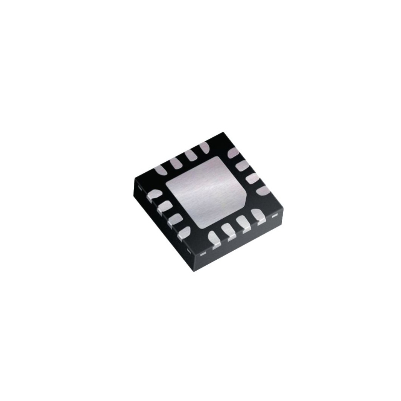
Package
The MC100EP195FAR2G chip package type is known as "QFN". It has a "16-LFCSP-VQFN" form and a size of 3.5mm x 3.5mm.

Datasheet PDF
We provide high quality products, thoughtful service and after sale guarantee
-

We have rich products, can meet your various needs.
-

Minimum order quantity starts from 1pcs.
-

Lowest international shipping fee starts from $0.00
-

365 days quality guarantee for all products