

Images are for reference only See Product Specifications
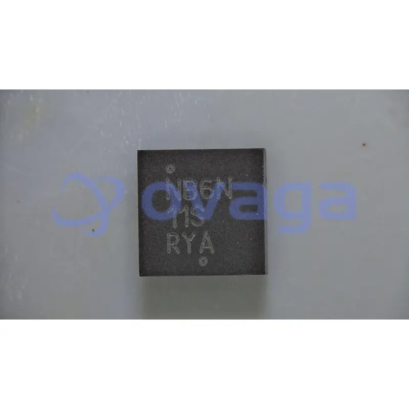
ON NB6N11SMNG
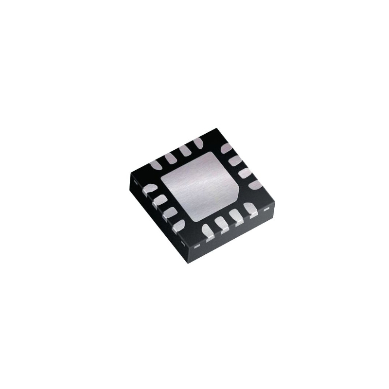
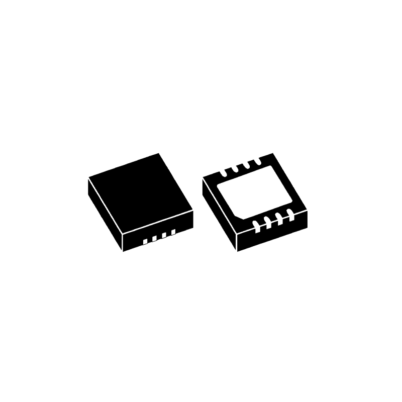
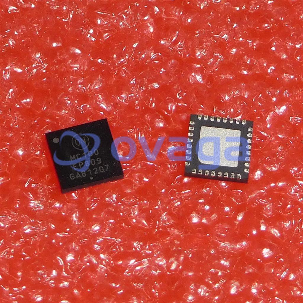
Clock Fanout Buffer (Distribution), Translator IC 1:2 2 GHz 16-VFQFN Exposed Pad


Brands: ON Semiconductor, LLC
Mfr.Part #: NB6N11SMNG
Datasheet: NB6N11SMNG Datasheet (PDF)
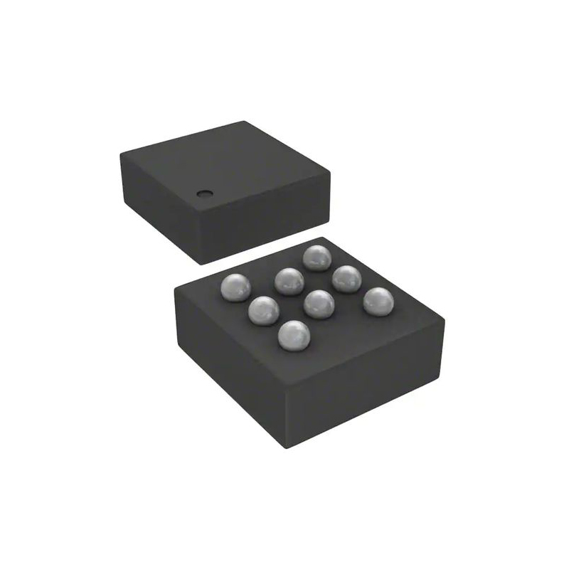
Package/Case: QFN-16 EP
Product Type: Clock & Timer ICs
NB6N11SMNG General Description
The NB6N11S is a differential 1:2 Clock or Data Receiver and will accept AnyLevelTM input signals: LVPECL, CML, LVCMOS, LVTTL, or LVDS. These signals will be translated to LVDS and two identical copies of Clock or Data will be distributed, operating up to 2.0 GHz or 2.5 Gb/s, respectively. As such, the NB6N11S is ideal for SONET, GigE, Fiber Channel, Backplane and other Clock or Data distribution applications. The NB6N11S has a wide input common mode range from GND + 50mV to VCC - 50 mV. Combined with the 50-ohm internal termination resistors at the inputs, the NB6N11S is ideal for translating a variety of differential or single-ended Clock or Data signals to 350 mV typical LVDS output levels. The NB6N11S is functionally equivalent to the EP11, LVEP11, SG11 or 7L11M devices and is offered in a small 3mm X 3mm 16-QFN package.
Features
- Maximum Input Clock Frequency > 2.0 GHz
- Maximum Input Data Rate > 2.5 Gb/s
- 1 ps Maximum of RMS Clock Jitter
- Typically 10 ps of Data Dependent Jitter
- 380 ps Typical Propagation Delay
- 120 ps Typical Rise and Fall Times
- These devices are available in Pb-free package(s). Specifications herein
Application
- High Performance LVDS Clock and Data Distribution for ATE and Networking
Specifications
| Parameter | Value | Parameter | Value |
|---|---|---|---|
| Source Content uid | NB6N11SMNG | Pbfree Code | Yes |
| Part Life Cycle Code | Active | Ihs Manufacturer | ONSEMI |
| Part Package Code | QFN16, 3x3, 0.5P | Package Description | QFN-16 |
| Pin Count | 16 | Manufacturer Package Code | 485G-01 |
| Reach Compliance Code | compliant | HTS Code | 8542.39.00.01 |
| Factory Lead Time | 39 Weeks | Samacsys Manufacturer | onsemi |
| Family | 6N | Input Conditioning | DIFFERENTIAL |
| JESD-30 Code | S-XQCC-N16 | Logic IC Type | LOW SKEW CLOCK DRIVER |
| Moisture Sensitivity Level | 1 | Number of Functions | 1 |
| Number of Inverted Outputs | Number of Terminals | 16 | |
| Number of True Outputs | 4 | Package Body Material | UNSPECIFIED |
| Package Code | HVQCCN | Package Equivalence Code | LCC16,.12SQ,20 |
| Package Shape | SQUARE | Package Style | CHIP CARRIER, HEAT SINK/SLUG, VERY THIN PROFILE |
| Peak Reflow Temperature (Cel) | 260 | Surface Mount | YES |
| Temperature Grade | INDUSTRIAL | Terminal Finish | NICKEL GOLD PALLADIUM |
| Terminal Form | NO LEAD | Terminal Position | QUAD |
| Time@Peak Reflow Temperature-Max (s) | 30 | feature-maximum-operating-supply-voltage-v | 3.6 |
| feature-minimum-operating-supply-voltage-v | 3 | feature-packaging | Rail |
| feature-rad-hard | feature-pin-count | 16 | |
| feature-supplier-package | QFN EP | feature-standard-package-name1 | QFN |
| feature-cecc-qualified | No | feature-esd-protection | Yes |
| feature-military | No | feature-aec-qualified | No |
| feature-aec-qualified-number | feature-auto-motive | No | |
| feature-p-pap | No | feature-eccn-code | EAR99 |
| feature-svhc | No |
Shipping
| Shipping Type | Ship Fee | Lead Time | |
|---|---|---|---|
 |
DHL | $20.00-$40.00 (0.50 KG) | 2-5 days |
 |
Fedex | $20.00-$40.00 (0.50 KG) | 2-5 days |
 |
UPS | $20.00-$40.00 (0.50 KG) | 2-5 days |
 |
TNT | $20.00-$40.00 (0.50 KG) | 2-5 days |
 |
EMS | $20.00-$40.00 (0.50 KG) | 2-5 days |
 |
REGISTERED AIR MAIL | $20.00-$40.00 (0.50 KG) | 2-5 days |
Processing Time:Shipping fee depend on different zone and country.
Payment
| Terms of payment | Hand Fee | |
|---|---|---|
 |
Wire Transfer | charge US$30.00 banking fee. |
 |
Paypal | charge 4.0% service fee. |
 |
Credit Card | charge 3.5% service fee. |
 |
Western Union | charge US.00 banking fee. |
 |
Money Gram | charge US$0.00 banking fee. |
Guarantees
1.The electronic components you purchase include 365 Days Warranty, We guarantee product quality.
2.If some of the items you received aren't of perfect quality, we would resiponsibly arrange your refund or replacement. But the items must remain their orginal condition.
Packing
-

Step1 :Product
-

Step2 :Vacuum packaging
-

Step3 :Anti-static bag
-

Step4 :Individual packaging
-

Step5 :Packaging boxes
-

Step6 :bar-code shipping tag
All the products will packing in anti-staticbag. Ship with ESD antistatic protection.
Outside ESD packing’s lable will use ourcompany’s information: Part Mumber, Brand and Quantity.
We will inspect all the goods before shipment,ensure all the products at good condition and ensure the parts are new originalmatch datasheet.
After all the goods are ensure no problems afterpacking, we will packing safely and send by global express. It exhibitsexcellent puncture and tear resistance along with good seal integrity.


Part points
-
The NB6N11SMNG is a high-performance clock driver chip designed specifically for applications requiring low phase noise and low voltage swing. It provides 6 output channels with programmable outputs enabling fine control over electrical characteristics. It operates at low power consumption and is suitable for various high-speed data communication systems.
-
Equivalent
Some equivalent products of the NB6N11SMNG chip include the NB6L11SMNG, NB6N14SMNG, and NB6N239SMNG. -
Features
The features of NB6N11SMNG include low power consumption, high speed performance, small size, and low output skew. It is a versatile clock and data buffer IC designed for use in networking, telecommunications, and other high-speed communication applications. -
Pinout
The NB6N11SMNG is a flat clock buffer with 1:2 Fanout. It has a pin count of 8 and functions as a high-performance clock distribution solution for demanding applications. -
Manufacturer
ON Semiconductor is the manufacturer of the NB6N11SMNG. It is a semiconductor manufacturing company that specializes in producing a wide range of electronic components, including integrated circuits and discrete devices. -
Application Field
The NB6N11SMNG is commonly used in various applications, including data communication, networking, and clock distribution systems. It can be found in routers, switches, data centers, and other electronic devices where precise and reliable clock synchronization is required. It helps ensure accurate data transmission and timing synchronization, making it an essential component in modern communication systems. -
Package
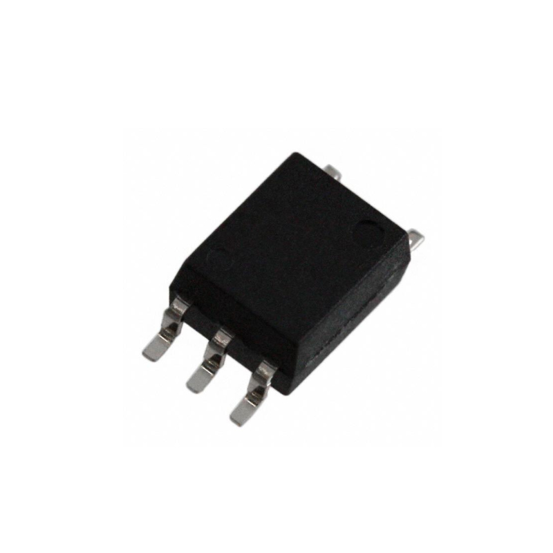
The NB6N11SMNG chip is available in a surface mount package with 8 leads. Its form factor is in a small outline integrated circuit (SOIC) package. The dimensions of the package are typically around 3.91mm x 4.90mm.
Datasheet PDF
We provide high quality products, thoughtful service and after sale guarantee
-

We have rich products, can meet your various needs.
-

Minimum order quantity starts from 1pcs.
-

Lowest international shipping fee starts from $0.00
-

365 days quality guarantee for all products
Excellent selection of components and competitive pricing. Thanks, Ovaga!