

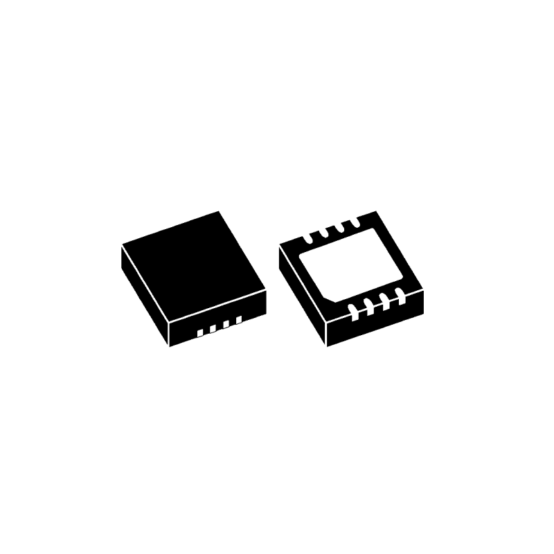
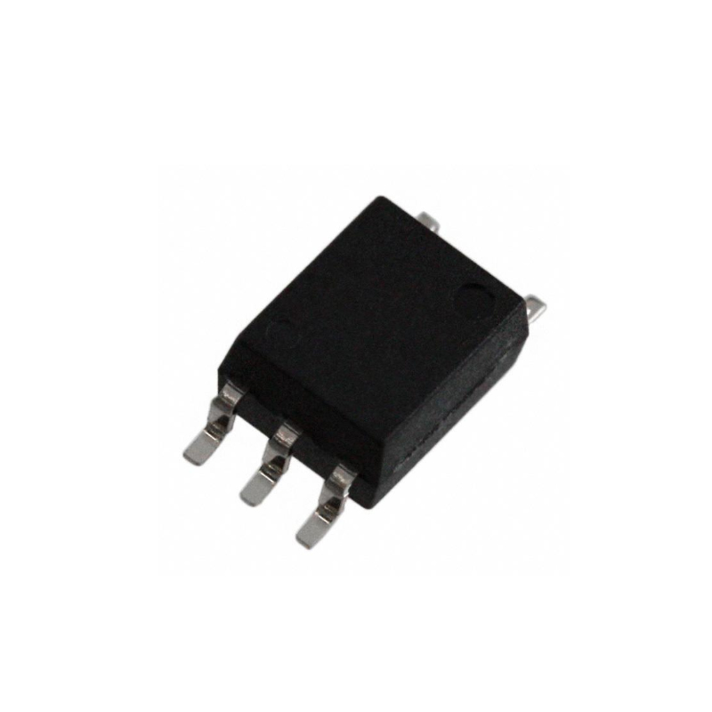
Images are for reference only See Product Specifications
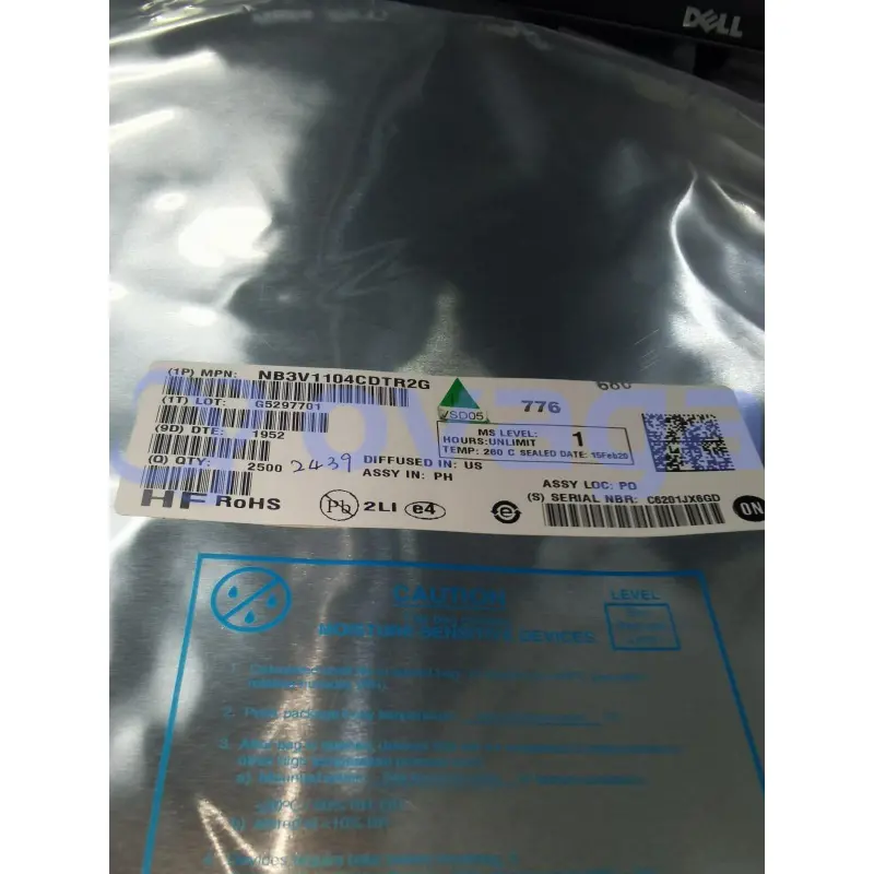
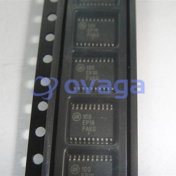
ON NB3V1104CDTR2G
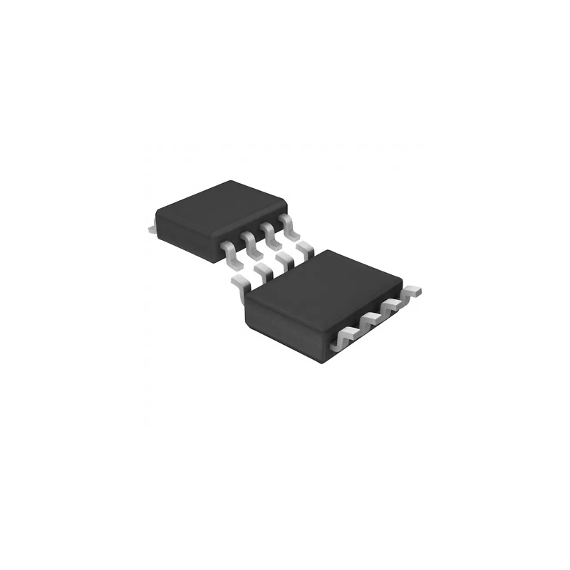
Clock Fanout Buffer (Distribution) IC 1:4 250 MHz 8-TSSOP (0.173", 4.40mm Width)


Brands: ON Semiconductor, LLC
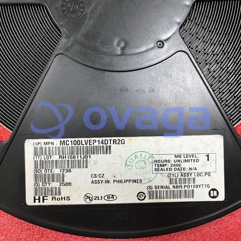
Mfr.Part #: NB3V1104CDTR2G
Datasheet: NB3V1104CDTR2G Datasheet (PDF)
Package/Case: TSSOP-8
RoHS Status:
Stock Condition: 2167 pcs, New Original
Product Type: Clock & Timer ICs
0
1
*All prices are in USD
| Qty | Unit Price | Ext Price |
|---|---|---|
| 1 | $2.267 | $2.267 |
| 10 | $1.960 | $19.600 |
| 30 | $1.768 | $53.040 |
| 100 | $1.572 | $157.200 |
| 500 | $1.483 | $741.500 |
| 1000 | $1.444 | $1444.000 |
In Stock:2167 PCS
NB3V1104CDTR2G General Description
The NB3V1104C is a member of the NB3V110xC a modular, high−performance, low−skew, general purpose LVCMOS clock buffer family. The device has a 1:4 fan-out. The family of devices is designed with a modular approach. Different fan-out variations, 1:2, 1:3, 1:4, 1:6 and 1:8, are available. All of the devices are pin compatible to each other for easy handling. All family members share the same high performing characteristics like low additive jitter, low skew, and wide operating temperature range. The NB3V110xCsupports an asynchronous output enable control (OE) which switchesthe outputs into a low state when OE is low. The NB3V110xC operatein a 3.3 V, 2.5 V and 1.8 V environment and are characterized for operation from –40°C to 105°C.
Features
- High−Performance 1:4 LVCMOS Clock Buffer
- Very Low Output−to−Output Skew < 50 ps
- Supply Voltage: 3.3 V, 2.5 V or 1.8 V
- Available in 8−Pin TSSOP
- Operating Temperature Range: –40°C to 105°C
- Low Additive Jitter
- fmax = 250 MHz for 3.3 V; fmax = 180 MHz for 2.5 V; fmax = 133 MHz for 1.8 V
- These Devices are Pb−Free and are RoHS Compliant
Application
- Clock Distribution
- Networking and Data Communication
- High-end Computing
Specifications
| Parameter | Value | Parameter | Value |
|---|---|---|---|
| Manufacturer: | ON Semiconductor | Product Category: | Clock Buffer |
| RoHS: | Y | Series: | NB3V110xC |
| Packaging: | Reel | Brand: | ON Semiconductor |
| Product Type: | Clock Buffer | Factory Pack Quantity: | 2500 |
| Subcategory: | Clock & Timer ICs | Tags | NB3V1, NB3V, NB3 |
| Source Content uid | NB3V1104CDTR2G | Pbfree Code | Yes |
| Part Life Cycle Code | Active | Ihs Manufacturer | ONSEMI |
| Package Description | TSSOP-14 | Manufacturer Package Code | 948S-01 |
| Reach Compliance Code | compliant | HTS Code | 8542.39.00.01 |
| Factory Lead Time | 71 Weeks | Samacsys Manufacturer | onsemi |
| Additional Feature | ALSO OPERATES AT 2.5V AND 3.3V VCC NOMINAL SUPPLY | Family | NB3V |
| Input Conditioning | STANDARD | JESD-30 Code | R-PDSO-G14 |
| Logic IC Type | LOW SKEW CLOCK DRIVER | Moisture Sensitivity Level | 1 |
| Number of Functions | 1 | Number of Inverted Outputs | |
| Number of Terminals | 14 | Number of True Outputs | 4 |
| Output Characteristics | 3-STATE | Package Body Material | PLASTIC/EPOXY |
| Package Code | TSSOP | Package Shape | RECTANGULAR |
| Package Style | SMALL OUTLINE, THIN PROFILE, SHRINK PITCH | Packing Method | TR |
| Peak Reflow Temperature (Cel) | 260 | Surface Mount | YES |
| Temperature Grade | INDUSTRIAL | Terminal Finish | NICKEL PALLADIUM GOLD |
| Terminal Form | GULL WING | Terminal Position | DUAL |
| Time@Peak Reflow Temperature-Max (s) | 30 |
Shipping
| Shipping Type | Ship Fee | Lead Time | |
|---|---|---|---|
 |
DHL | $20.00-$40.00 (0.50 KG) | 2-5 days |
 |
Fedex | $20.00-$40.00 (0.50 KG) | 2-5 days |
 |
UPS | $20.00-$40.00 (0.50 KG) | 2-5 days |
 |
TNT | $20.00-$40.00 (0.50 KG) | 2-5 days |
 |
EMS | $20.00-$40.00 (0.50 KG) | 2-5 days |
 |
REGISTERED AIR MAIL | $20.00-$40.00 (0.50 KG) | 2-5 days |
Processing Time:Shipping fee depend on different zone and country.
Payment
| Terms of payment | Hand Fee | |
|---|---|---|
 |
Wire Transfer | charge US$30.00 banking fee. |
 |
Paypal | charge 4.0% service fee. |
 |
Credit Card | charge 3.5% service fee. |
 |
Western Union | charge US.00 banking fee. |
 |
Money Gram | charge US$0.00 banking fee. |
Guarantees
1.The electronic components you purchase include 365 Days Warranty, We guarantee product quality.
2.If some of the items you received aren't of perfect quality, we would resiponsibly arrange your refund or replacement. But the items must remain their orginal condition.
Packing
-

Step1 :Product
-

Step2 :Vacuum packaging
-

Step3 :Anti-static bag
-

Step4 :Individual packaging
-

Step5 :Packaging boxes
-

Step6 :bar-code shipping tag
All the products will packing in anti-staticbag. Ship with ESD antistatic protection.
Outside ESD packing’s lable will use ourcompany’s information: Part Mumber, Brand and Quantity.
We will inspect all the goods before shipment,ensure all the products at good condition and ensure the parts are new originalmatch datasheet.
After all the goods are ensure no problems afterpacking, we will packing safely and send by global express. It exhibitsexcellent puncture and tear resistance along with good seal integrity.


Part points
-
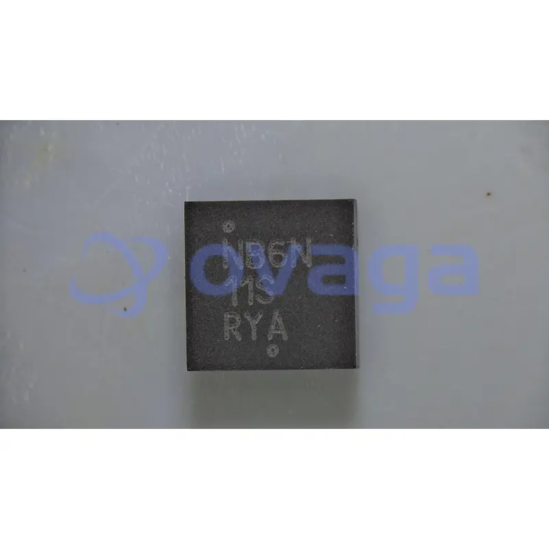
The NB3V1104CDTR2G chip is a voltage controlled oscillator (VCO) designed for low phase noise applications. It operates at a frequency range of 150MHz to 190MHz and provides an output in the form of a square wave. This chip is commonly used in communication systems, radio frequency (RF) equipment, and wireless devices to generate stable and accurate clock signals.
-
Features
Features of NB3V1104CDTR2G include a low power consumption of 3 µA, a wide voltage supply range of 1.65V to 5.5V, a compact size of 1.2 x 1.2 mm, a wide temperature range of -40°C to +85°C, and a stable operation with low jitter. It also offers a 2.5V compatibility and supports I2C interface. -
Pinout
The NB3V1104CDTR2G is a 1:4 clock buffer with a pin count of 16. Its functions include voltage level translation, clock distribution, and clock signal buffering for various applications. -
Manufacturer
The manufacturer of the NB3V1104CDTR2G is ON Semiconductor. ON Semiconductor is a multinational semiconductor manufacturing company that specializes in a wide range of products, including power management, signal conditioning, custom devices, and standard components. They provide innovative solutions for various industries, including automotive, industrial, communication, and consumer electronics. -
Application Field
The NB3V1104CDTR2G is a high-speed clock and data recovery IC designed for applications that require data transfer over long distances. It is commonly used in optical communication systems, fiber-optic networks, and high-speed data transmission applications in telecommunications and networking. -
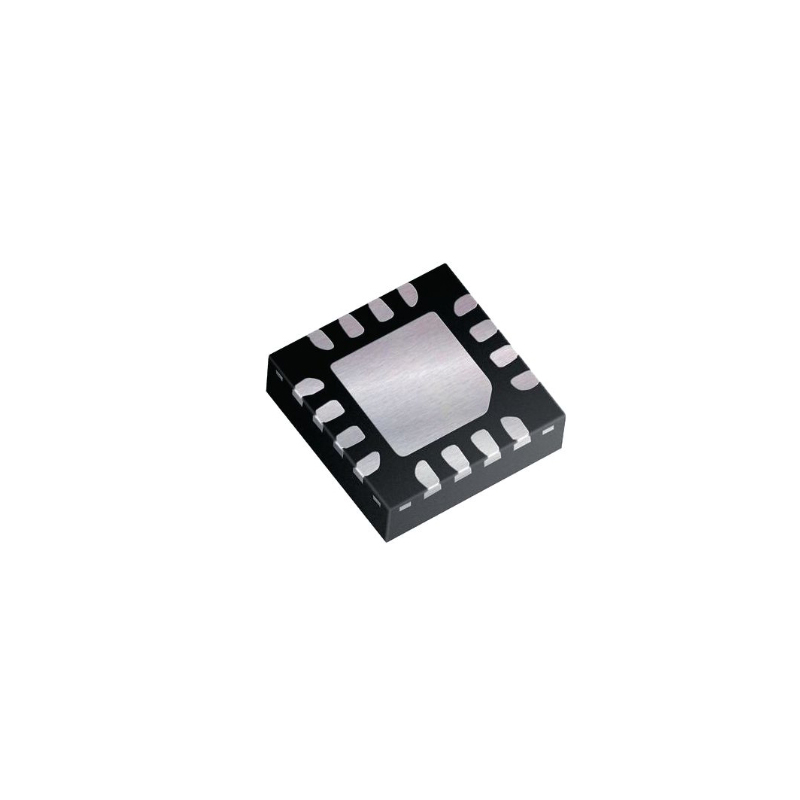
Package
The NB3V1104CDTR2G chip is available in a package type called DFN-6 (Dual Flat No-Lead). It has a form factor of 3mm x 3mm and a size of approximately 15.4mm².
Datasheet PDF
We provide high quality products, thoughtful service and after sale guarantee
-

We have rich products, can meet your various needs.
-

Minimum order quantity starts from 1pcs.
-

Lowest international shipping fee starts from $0.00
-

365 days quality guarantee for all products
Ratings and Reviews
Ovaga's website is easy to use and their selection of electronic components is unparalleled.
Average products, but quick shipping.