


Images are for reference only See Product Specifications
ON FDMS3669S
MOSFET 30V Asymmetric Dual N-Channel Pwr Trench


Brands: ON Semiconductor, LLC
Mfr.Part #: FDMS3669S
Datasheet: FDMS3669S Datasheet (PDF)
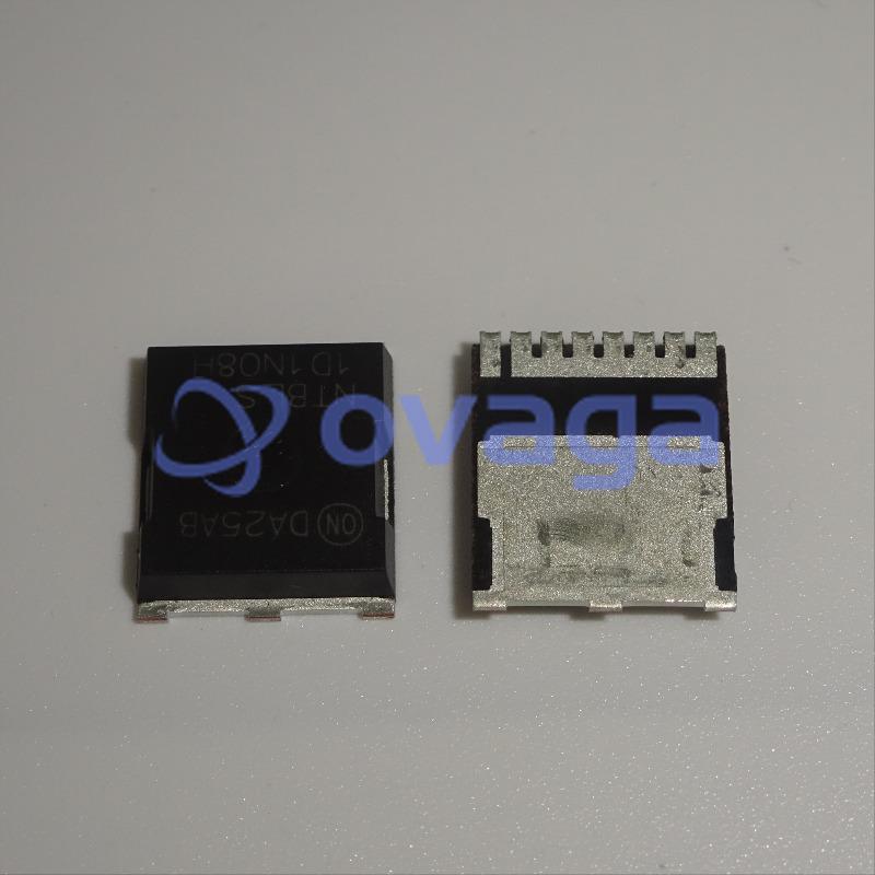
Package/Case: Power 56
Product Type: Transistors
FDMS3669S General Description
This device includes two specialized N-Channel MOSFETs in a dual PQFN package. The switch node has been internally connected to enable easy placement and routing of synchronous buck converters. The control MOSFET (Q1) and synchronousSyncFET™ (Q2) have been designed to provide optimal power efficiency.
Features
- Q1: N-Channel
Max rDS(on) = 10 mΩ at VGS = 10 V, ID = 13 A
Max rDS(on) = 14.5 mΩ at VGS = 4.5 V, ID = 10 A - Q2: N-Channel
Max rDS(on) = 5 mΩ at VGS = 10 V, ID = 18 A
Max rDS(on) = 5.2 mΩ at VGS = 4.5 V, ID = 17 A - Low inductance packaging shortens rise/fall times, resulting in lower switching losses
- MOSFET integration enables optimum layout for lower circuit inductance and reduced switch node ringing
- RoHS Compliant
Application
- Notebook PC
Specifications
| Parameter | Value | Parameter | Value |
|---|---|---|---|
| Source Content uid | FDMS3669S | Pbfree Code | Yes |
| Part Life Cycle Code | Active | Ihs Manufacturer | ONSEMI |
| Package Description | QFN-8 | Manufacturer Package Code | 483AJ |
| Reach Compliance Code | not_compliant | ECCN Code | EAR99 |
| HTS Code | 8541.29.00.95 | Factory Lead Time | 54 Weeks |
| Samacsys Manufacturer | onsemi | Case Connection | DRAIN SOURCE |
| Configuration | SERIES, 2 ELEMENTS WITH BUILT-IN DIODE | DS Breakdown Voltage-Min | 30 V |
| Drain Current-Max (ID) | 13 A | Drain-source On Resistance-Max | 0.01 Ω |
| FET Technology | METAL-OXIDE SEMICONDUCTOR | Feedback Cap-Max (Crss) | 55 pF |
| JEDEC-95 Code | MO-240AA | JESD-30 Code | R-PDSO-F6 |
| JESD-609 Code | e3 | Moisture Sensitivity Level | 1 |
| Number of Elements | 2 | Number of Terminals | 6 |
| Operating Mode | ENHANCEMENT MODE | Operating Temperature-Max | 150 °C |
| Operating Temperature-Min | -55 °C | Package Body Material | PLASTIC/EPOXY |
| Package Shape | RECTANGULAR | Package Style | SMALL OUTLINE |
| Peak Reflow Temperature (Cel) | 260 | Polarity/Channel Type | N-CHANNEL |
| Power Dissipation Ambient-Max | 2.5 W | Power Dissipation-Max (Abs) | 2.5 W |
| Surface Mount | YES | Terminal Finish | Matte Tin (Sn) - annealed |
| Terminal Form | FLAT | Terminal Position | DUAL |
| Time@Peak Reflow Temperature-Max (s) | 30 | Transistor Application | SWITCHING |
| Transistor Element Material | SILICON |
Shipping
| Shipping Type | Ship Fee | Lead Time | |
|---|---|---|---|
 |
DHL | $20.00-$40.00 (0.50 KG) | 2-5 days |
 |
Fedex | $20.00-$40.00 (0.50 KG) | 2-5 days |
 |
UPS | $20.00-$40.00 (0.50 KG) | 2-5 days |
 |
TNT | $20.00-$40.00 (0.50 KG) | 2-5 days |
 |
EMS | $20.00-$40.00 (0.50 KG) | 2-5 days |
 |
REGISTERED AIR MAIL | $20.00-$40.00 (0.50 KG) | 2-5 days |
Processing Time:Shipping fee depend on different zone and country.
Payment
| Terms of payment | Hand Fee | |
|---|---|---|
 |
Wire Transfer | charge US$30.00 banking fee. |
 |
Paypal | charge 4.0% service fee. |
 |
Credit Card | charge 3.5% service fee. |
 |
Western Union | charge US.00 banking fee. |
 |
Money Gram | charge US$0.00 banking fee. |
Guarantees
1.The electronic components you purchase include 365 Days Warranty, We guarantee product quality.
2.If some of the items you received aren't of perfect quality, we would resiponsibly arrange your refund or replacement. But the items must remain their orginal condition.
Packing
-

Step1 :Product
-

Step2 :Vacuum packaging
-

Step3 :Anti-static bag
-

Step4 :Individual packaging
-

Step5 :Packaging boxes
-

Step6 :bar-code shipping tag
All the products will packing in anti-staticbag. Ship with ESD antistatic protection.
Outside ESD packing’s lable will use ourcompany’s information: Part Mumber, Brand and Quantity.
We will inspect all the goods before shipment,ensure all the products at good condition and ensure the parts are new originalmatch datasheet.
After all the goods are ensure no problems afterpacking, we will packing safely and send by global express. It exhibitsexcellent puncture and tear resistance along with good seal integrity.


Part points
-
FDMS3669S is a power MOSFET (metal-oxide-semiconductor field-effect transistor) chip commonly used in electronic devices. It is known for its efficient power management and low on-resistance, allowing for high-performance operation while minimizing power loss. The chip is designed to improve the overall power efficiency of electronic systems, making it suitable for applications such as mobile devices, laptops, and various consumer electronics.
-
Equivalent
The equivalent products of the FDMS3669S chip include the AON6428, AON6418, and AON6403. -
Features
The FDMS3669S is a power MOSFET that has a maximum drain-source voltage rating of 30V and a maximum drain current rating of 80A. It features a low on-resistance, fast switching speed, and a compact surface-mount package. It is commonly used in applications such as power supplies, motor control, and automotive systems. -
Pinout
The FDMS3669S is a dual N-channel PowerTrench® MOSFET. Its pin count is 8, with 4 pins for each MOSFET: drain (D), source (S), gate (G), and body (B). This MOSFET is used for power management applications and provides low on-resistance and high power density. -
Manufacturer
The manufacturer of the FDMS3669S is Fairchild Semiconductor. It is a semiconductor manufacturing company that specializes in the design, development, and production of integrated circuits and power devices for various industries, including automotive, consumer electronics, and industrial applications. -
Application Field
The FDMS3669S is a power stage module designed for DC-DC applications. Some application areas include power distribution systems, telecommunications, industrial equipment, automotive, and consumer electronics where high power density and efficiency are required. It is commonly used in power management systems for voltage regulation and conversion purposes. -
Package
The FDMS3669S chip is in a Power56 package type, with a form that is surface mount. Its size is 8.88mm x 7.06mm.
Datasheet PDF
We provide high quality products, thoughtful service and after sale guarantee
-

We have rich products, can meet your various needs.
-

Minimum order quantity starts from 1pcs.
-

Lowest international shipping fee starts from $0.00
-

365 days quality guarantee for all products

Components worked fine, no issues there.