

Images are for reference only See Product Specifications
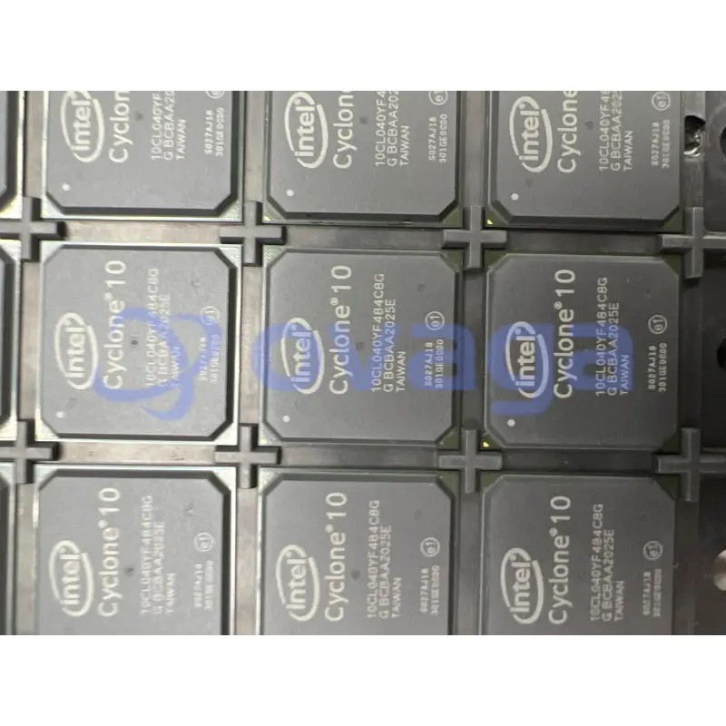
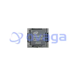
Intel 10CL040YF484C8G
FPGA Cyclone® 10 LP Family 39600 Cells 484-Pin FBGA Tray


Brands: Intel
Mfr.Part #: 10CL040YF484C8G
Datasheet: 10CL040YF484C8G Datasheet (PDF)
Package/Case: FBGA-484
Product Type: FPGA - Field Programmable Gate Array
RoHS Status:
Stock Condition: 9458 pcs, New Original
Warranty: 1 Year Ovaga Warranty - Find Out More
0
1
Add To Bom10CL040YF484C8G General Description
Cyclone® 10 LP Field Programmable Gate Array (FPGA) IC 325 1161216 39600 484-BGA
Features
- Metal case with ceramic insulator International standard case TO-200AC (B-PUK) All diffused design Center amplifying gate Guaranteed high dV/dt Guaranteed high dI/dt High surge current capibility Low thermal impedance High speed performance

Specifications
| Parameter | Value | Parameter | Value |
|---|---|---|---|
| Manufacturer: | Intel | Product Category: | FPGA - Field Programmable Gate Array |
| RoHS: | Details | Series: | Cyclone 10 LP 10CL040 |
| Number of Logic Elements: | 39600 LE | Adaptive Logic Modules - ALMs: | - |
| Embedded Memory: | 1134 kbit | Number of I/Os: | 325 I/O |
| Supply Voltage - Min: | 1.2 V | Supply Voltage - Max: | 1.2 V |
| Minimum Operating Temperature: | 0 C | Maximum Operating Temperature: | + 85 C |
| Data Rate: | - | Number of Transceivers: | - |
| Mounting Style: | SMD/SMT | Package / Case: | FBGA-484 |
| Packaging: | Tray | Brand: | Intel / Altera |
| Maximum Operating Frequency: | - | Moisture Sensitive: | Yes |
| Number of Logic Array Blocks - LABs: | 2475 LAB | Operating Supply Voltage: | 1.2 V |
| Product Type: | FPGA - Field Programmable Gate Array | Factory Pack Quantity: | 60 |
| Subcategory: | Programmable Logic ICs | Tradename: | Cyclone |
| Part # Aliases: | 973651 |
Shipping
| Shipping Type | Ship Fee | Lead Time | |
|---|---|---|---|
 |
DHL | $20.00-$40.00 (0.50 KG) | 2-5 days |
 |
Fedex | $20.00-$40.00 (0.50 KG) | 2-5 days |
 |
UPS | $20.00-$40.00 (0.50 KG) | 2-5 days |
 |
TNT | $20.00-$40.00 (0.50 KG) | 2-5 days |
 |
EMS | $20.00-$40.00 (0.50 KG) | 2-5 days |
 |
REGISTERED AIR MAIL | $20.00-$40.00 (0.50 KG) | 2-5 days |
Processing Time:Shipping fee depend on different zone and country.
Payment
| Terms of payment | Hand Fee | |
|---|---|---|
 |
Wire Transfer | charge US$30.00 banking fee. |
 |
Paypal | charge 4.0% service fee. |
 |
Credit Card | charge 3.5% service fee. |
 |
Western Union | charge US.00 banking fee. |
 |
Money Gram | charge US$0.00 banking fee. |
Guarantees
1.The electronic components you purchase include 365 Days Warranty, We guarantee product quality.
2.If some of the items you received aren't of perfect quality, we would resiponsibly arrange your refund or replacement. But the items must remain their orginal condition.
Packing
-

Step1 :Product
-

Step2 :Vacuum packaging
-

Step3 :Anti-static bag
-

Step4 :Individual packaging
-

Step5 :Packaging boxes
-

Step6 :bar-code shipping tag


All the products will packing in anti-staticbag. Ship with ESD antistatic protection.
Outside ESD packing’s lable will use ourcompany’s information: Part Mumber, Brand and Quantity.
We will inspect all the goods before shipment,ensure all the products at good condition and ensure the parts are new originalmatch datasheet.
After all the goods are ensure no problems afterpacking, we will packing safely and send by global express. It exhibitsexcellent puncture and tear resistance along with good seal integrity.


Part points
-
The 10CL040YF484C8G chip is a programmable logic device (PLD) designed by Intel. It features 40,000 logic elements and supports high-speed data transmission capabilities. This chip is commonly used in various applications, such as industrial automation, telecommunications, and digital signal processing. It allows for the implementation of complex logic functions and offers a wide range of configuration options to tailor it to specific requirements.
-
Equivalent
There are no direct equivalent products to the 10CL040YF484C8G chip as it is a specific model and designation. However, there may be similar FPGA chips from the same manufacturer or other manufacturers that provide similar functionalities and specifications. -
Features
The 10CL040YF484C8G is an FPGA (Field-Programmable Gate Array) device from Intel (formerly Altera). It features 40,160 logic elements, high-speed transceivers, embedded memory, digital signal processing (DSP) blocks, and supports various I/O interfaces. It is designed for advanced applications that require high-performance and versatility in a compact form factor. -
Pinout
The pin count of the 10CL040YF484C8G is 484. The function of the device would depend on its specific application or usage, as it is an FPGA product. FPGAs (Field-Programmable Gate Arrays) are integrated circuits that can be programmed to perform various digital logic functions, depending on the user's requirements. -
Manufacturer
Xilinx is the manufacturer of the 10CL040YF484C8G. Xilinx is a multinational technology company specializing in designing and producing programmable logic devices and related software development systems. They are known for their field-programmable gate arrays (FPGAs) and systems on chips (SoCs). -
Application Field
The 10CL040YF484C8G is a Field-Programmable Gate Array (FPGA) chip that can be used in various application areas such as telecommunications, automotive, industrial automation, aerospace, and defense. Its high performance and flexibility make it suitable for applications requiring high-speed data processing, signal processing, and control functions. -
Package
The 10CL040YF484C8G chip is packaged in a plastic flip-chip Ball Grid Array (BGA) with a size of 19x19mm.


We provide high quality products, thoughtful service and after sale guarantee
-

We have rich products, can meet your various needs.
-

Minimum order quantity starts from 1pcs.
-

Lowest international shipping fee starts from $0.00
-

365 days quality guarantee for all products


