


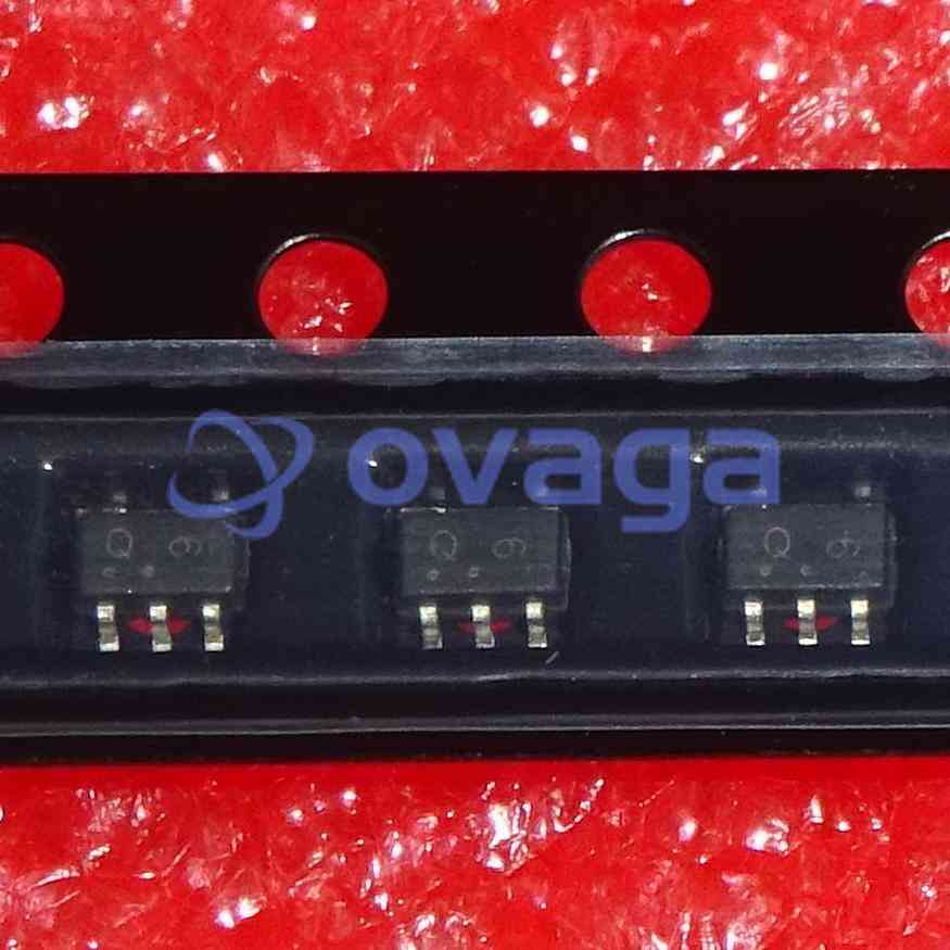
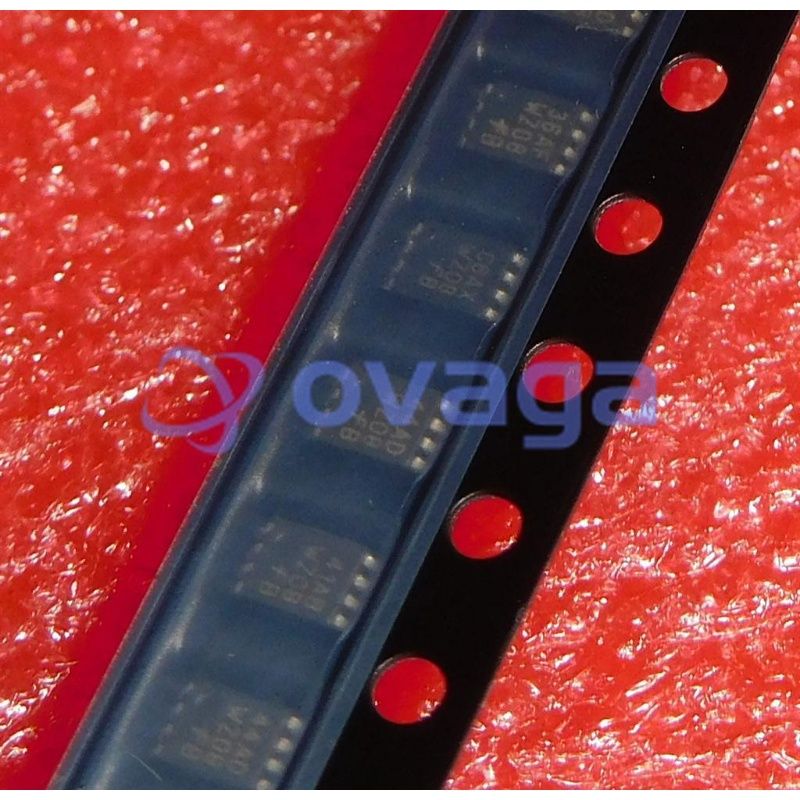
Images are for reference only See Product Specifications
ON MC14094BDR2G
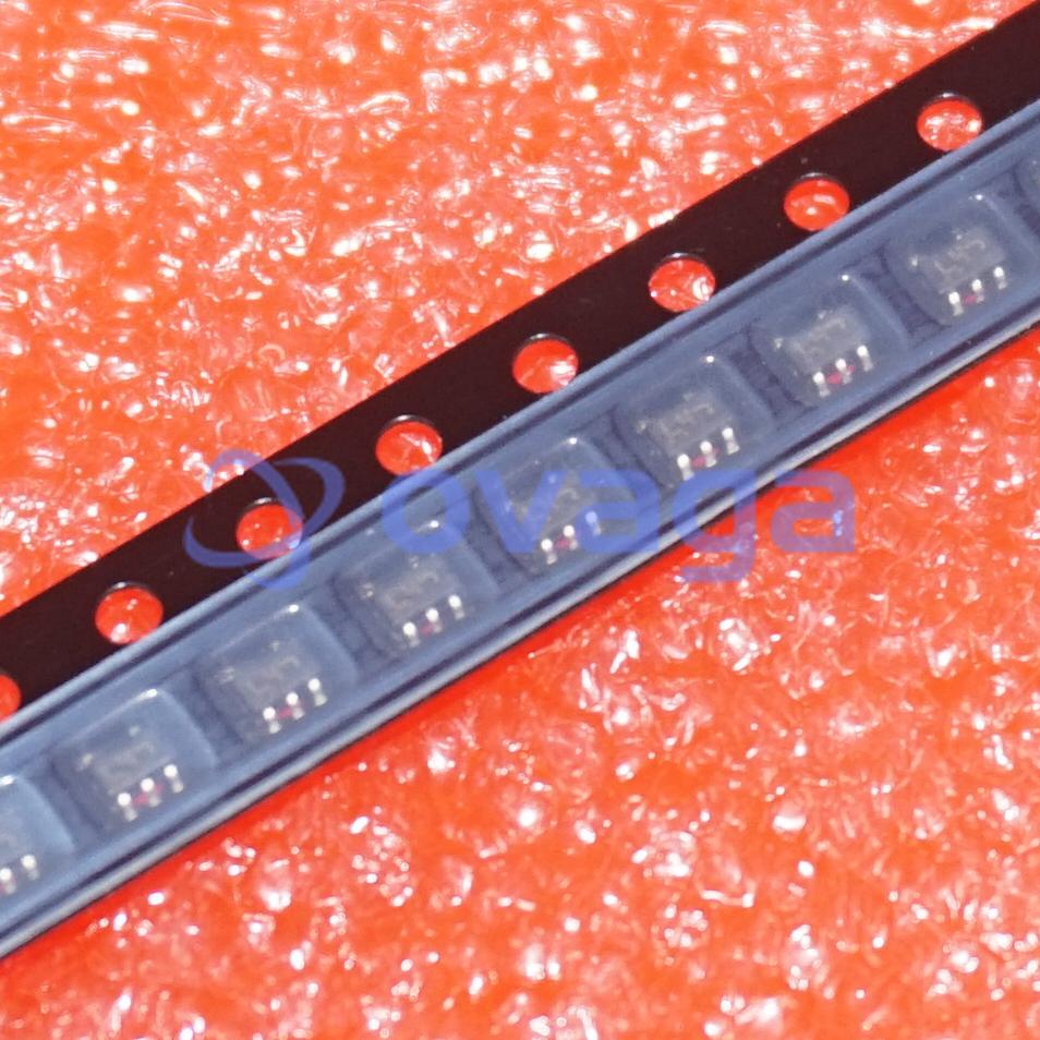
Shift Shift Register 1 Element 8 Bit 16-SOIC


Brands: ON Semiconductor, LLC
Mfr.Part #: MC14094BDR2G
Datasheet: MC14094BDR2G Datasheet (PDF)
Package/Case: SOIC-16
RoHS Status:
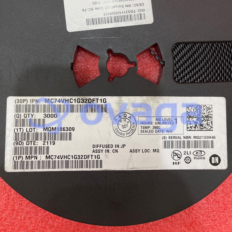
Stock Condition: 3502 pcs, New Original
Product Type: Logic ICs
0
1
*All prices are in USD
| Qty | Unit Price | Ext Price |
|---|---|---|
| 1 | $0.477 | $0.477 |
| 10 | $0.389 | $3.890 |
| 30 | $0.346 | $10.380 |
| 100 | $0.301 | $30.100 |
| 500 | $0.270 | $135.000 |
| 1000 | $0.256 | $256.000 |
In Stock:3502 PCS
MC14094BDR2G General Description
The MC14094B combines an 8-stage shift register with a data latch for each stage and a three-state output from each latch.
Data is shifted on the positive clock transition and is shifted from the seventh stage to two serial outputs. The QS output data is for use in high-speed cascaded systems. The Q S output data is shifted on the following negative clock transition for use in low-speed cascaded systems.
Data from each stage of the shift register is latched on the negative transition of the strobe input. Data propagates through the latch while strobe is high.
Outputs of the eight data latches are controlled by three-state buffers which are placed in the high-impedance state by a logic Low on Output Enable.
Features
- Three-State Outputs
- Capable of Driving Two Low-Power TTL Loads or One Low-Power Schottky TTL Load Over the Rated Temperature Range
- Input Diode Protection
- Data Latch
- Dual Outputs for Data Out on Both Positive and Negative Clock Transitions
- Useful for Serial-to-Parallel Data Conversion
- Pin-for-Pin Compatible with CD4094B
- Pb-Free Packages are Available*
Application
ONSEMISpecifications
| Parameter | Value | Parameter | Value |
|---|---|---|---|
| Source Content uid | MC14094BDR2G | Pbfree Code | Yes |
| Part Life Cycle Code | Active | Ihs Manufacturer | ONSEMI |
| Part Package Code | SOIC 16 LEAD | Pin Count | 16 |
| Manufacturer Package Code | 751B-05 | Reach Compliance Code | compliant |
| HTS Code | 8542.39.00.01 | Factory Lead Time | 40 Weeks |
| Samacsys Manufacturer | onsemi | Family | 4000/14000/40000 |
| JESD-30 Code | R-PDSO-G16 | Logic IC Type | SERIAL IN PARALLEL OUT |
| Moisture Sensitivity Level | 1 | Number of Bits | 8 |
| Number of Functions | 1 | Number of Terminals | 16 |
| Output Characteristics | 3-STATE | Output Polarity | TRUE |
| Package Body Material | PLASTIC/EPOXY | Package Code | SOP |
| Package Equivalence Code | SOP16,.25 | Package Shape | RECTANGULAR |
| Package Style | SMALL OUTLINE | Peak Reflow Temperature (Cel) | 260 |
| Surface Mount | YES | Technology | CMOS |
| Temperature Grade | MILITARY | Terminal Finish | MATTE TIN |
| Terminal Form | GULL WING | Terminal Position | DUAL |
| Time@Peak Reflow Temperature-Max (s) | 30 | Trigger Type | POSITIVE EDGE |
| feature-logic-family | 4000 | feature-logic-function | Shift Register/Latch |
| feature-number-of-elements-per-chip | 1 | feature-process-technology | CMOS |
| feature-maximum-low-level-output-current-ma | feature-output-type | 3-State | |
| feature-minimum-operating-supply-voltage-v | 3 | feature-maximum-operating-supply-voltage-v | 18 |
| feature-maximum-high-level-output-current-ma | feature-packaging | Tape and Reel | |
| feature-rad-hard | feature-pin-count | 16 | |
| feature-supplier-package | SOIC | feature-standard-package-name1 | SO |
| feature-cecc-qualified | No | feature-esd-protection | |
| feature-military | No | feature-aec-qualified | No |
| feature-aec-qualified-number | feature-auto-motive | No | |
| feature-p-pap | No | feature-eccn-code | EAR99 |
| feature-svhc | No |
Shipping
| Shipping Type | Ship Fee | Lead Time | |
|---|---|---|---|
 |
DHL | $20.00-$40.00 (0.50 KG) | 2-5 days |
 |
Fedex | $20.00-$40.00 (0.50 KG) | 2-5 days |
 |
UPS | $20.00-$40.00 (0.50 KG) | 2-5 days |
 |
TNT | $20.00-$40.00 (0.50 KG) | 2-5 days |
 |
EMS | $20.00-$40.00 (0.50 KG) | 2-5 days |
 |
REGISTERED AIR MAIL | $20.00-$40.00 (0.50 KG) | 2-5 days |
Processing Time:Shipping fee depend on different zone and country.
Payment
| Terms of payment | Hand Fee | |
|---|---|---|
 |
Wire Transfer | charge US$30.00 banking fee. |
 |
Paypal | charge 4.0% service fee. |
 |
Credit Card | charge 3.5% service fee. |
 |
Western Union | charge US.00 banking fee. |
 |
Money Gram | charge US$0.00 banking fee. |
Guarantees
1.The electronic components you purchase include 365 Days Warranty, We guarantee product quality.
2.If some of the items you received aren't of perfect quality, we would resiponsibly arrange your refund or replacement. But the items must remain their orginal condition.
Packing
-

Step1 :Product
-

Step2 :Vacuum packaging
-

Step3 :Anti-static bag
-

Step4 :Individual packaging
-

Step5 :Packaging boxes
-

Step6 :bar-code shipping tag
All the products will packing in anti-staticbag. Ship with ESD antistatic protection.
Outside ESD packing’s lable will use ourcompany’s information: Part Mumber, Brand and Quantity.
We will inspect all the goods before shipment,ensure all the products at good condition and ensure the parts are new originalmatch datasheet.
After all the goods are ensure no problems afterpacking, we will packing safely and send by global express. It exhibitsexcellent puncture and tear resistance along with good seal integrity.


Part points
-
The MC14094BDR2G chip is a CMOS hex Schmitt trigger designed for general-purpose digital logic applications. It features hysteresis to improve noise immunity and has a wide supply voltage range. The chip has six Schmitt trigger inputs and outputs, making it suitable for various applications such as signal conditioning, debouncing, and waveform shaping. It is commonly used in communication systems, industrial equipment, and automotive electronics.
-
Equivalent
Some potential equivalent products to the MC14094BDR2G chip include the CD4094B, 74HC594, and TC4094BP. -
Features
MC14094BDR2G is a hex Schmitt trigger with Schmitt trigger inputs. It offers hysteresis voltage to improve noise immunity and robustness. This device includes 4000B series buffered outputs, providing high noise immunity and stable output. The device is intended for interfacing between digital systems and general-purpose digital systems. -
Pinout
The MC14094BDR2G is a 14-pin, hex inverter buffer IC. It is commonly used for various digital logic applications. The pin count and function details are as follows: - Pin 1: Input A1 - Pin 2: Output B1 - Pin 3: Enable A - Pin 4: Output B - Pin 5: Input A - Pin 6: Ground (GND) - Pin 7: Output C - Pin 8: Output D - Pin 9: Input C - Pin 10: Output E - Pin 11: Output F - Pin 12: Input D - Pin 13: VDD (Positive power supply) - Pin 14: Input E -
Manufacturer
The manufacturer of the MC14094BDR2G is ON Semiconductor. It is a multinational semiconductor supplier company that specializes in power management, sensing, and connectivity solutions. -
Application Field
The MC14094BDR2G is a Hex Schmitt Trigger integrated circuit. It can be used in various applications, including waveform shaping, debounce circuits, pulse shaping, and digital logic implementation. -
Package
The MC14094BDR2G chip is packaged in a SOIC (Small Outline Integrated Circuit) package, with 14 pins. The chip measures approximately 8.75mm x 3.91mm x 1.75mm (L x W x H).
Datasheet PDF
We provide high quality products, thoughtful service and after sale guarantee
-

We have rich products, can meet your various needs.
-

Minimum order quantity starts from 1pcs.
-

Lowest international shipping fee starts from $0.00
-

365 days quality guarantee for all products
Exceptional service and exceptional components - what more could you ask for?