Images are for reference only See Product Specifications
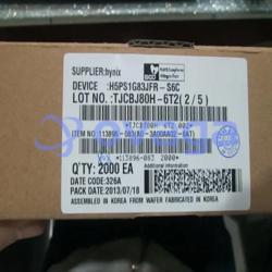
H5PS5162GFR-S5C
DDR DRAM, 32MX16, 0.4ns, CMOS, PBGA84, 7.50 X 12.50 MM, HALOGEN FREE AND ROHS COMPLIANT, FBGA-84


Brands: SK HYNIX INC
Mfr.Part #: H5PS5162GFR-S5C
Datasheet: H5PS5162GFR-S5C Datasheet (PDF)
Package/Case: FBGA-84
Product Type: DRAMs
RoHS Status:
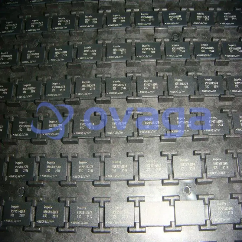
Stock Condition: 6554 pcs, New Original
Warranty: 1 Year Ovaga Warranty - Find Out More
0
1
Add To Bom
Features
- VDD = 1.8 +/- 0.1V
- VDDQ = 1.8 +/- 0.1V
- All inputs and outputs are compatible with SSTL_18 interface
- 8 banks
- Fully differential clock inputs (CK, /CK) operation
- Double data rate interface
- Source synchronous-data transaction aligned to bidirectional data strobe (DQS, DQS)
- Differential Data Strobe (DQS, DQS)
- Data outputs on DQS, DQSedges when read (edged DQ)
- Data inputs on DQS centers when write (centered DQ)
- On chip DLL align DQ, DQS and DQStransition with CK transition
- DM mask write data-in at the both rising and falling edges of the data strobe
- All addresses and control inputs except data, data strobes and data masks latched on the rising
- edges of the clock
- Programmable CAS latency 3, 4, 5 and 6 supported
- Programmable additive latency 0, 1, 2, 3, 4 and 5 supported
- Programmable burst length 4/8 with bothnibble sequential and interleave mode
- Internal eight bank operations with single pulsed RAS
- Auto refresh and self refresh supported
- tRAS lockout supported
- 8K refresh cycles /64ms
- JEDEC standard 60ball FBGA(x4/x8), 84ball FBGA(x16)
- Full strength driver option controlled by EMR
- On Die Termination supported
- Off Chip Driver Impedance Adjustment supported
- Read Data Strobe supported (x8 only)
- Self-Refresh High Temperature Entry
Specifications
| Parameter | Value | Parameter | Value |
|---|---|---|---|
| Rohs Code | Yes | Part Life Cycle Code | Obsolete |
| Ihs Manufacturer | SK HYNIX INC | Part Package Code | BGA |
| Package Description | TFBGA, BGA84,9X15,32 | Pin Count | 84 |
| Reach Compliance Code | ECCN Code | EAR99 | |
| HTS Code | 8542.32.00.28 | Access Mode | FOUR BANK PAGE BURST |
| Access Time-Max | 0.4 ns | Additional Feature | AUTO/SELF REFRESH |
| Clock Frequency-Max (fCLK) | 400 MHz | I/O Type | COMMON |
| Interleaved Burst Length | 4,8 | JESD-30 Code | R-PBGA-B84 |
| JESD-609 Code | e1 | Length | 12.5 mm |
| Memory Density | 536870912 bit | Memory IC Type | DDR2 DRAM |
| Memory Width | 16 | Number of Functions | 1 |
| Number of Ports | 1 | Number of Terminals | 84 |
| Number of Words | 33554432 words | Number of Words Code | 32000000 |
| Operating Mode | SYNCHRONOUS | Operating Temperature-Max | 95 °C |
| Operating Temperature-Min | Organization | 32MX16 | |
| Output Characteristics | 3-STATE | Package Body Material | PLASTIC/EPOXY |
| Package Code | TFBGA | Package Equivalence Code | BGA84,9X15,32 |
| Package Shape | RECTANGULAR | Package Style | GRID ARRAY, THIN PROFILE, FINE PITCH |
| Peak Reflow Temperature (Cel) | 260 | Power Supplies | 1.8 V |
| Qualification Status | Not Qualified | Refresh Cycles | 8192 |
| Seated Height-Max | 1.2 mm | Self Refresh | YES |
| Sequential Burst Length | 4,8 | Standby Current-Max | 0.007 A |
| Supply Current-Max | 0.184 mA | Supply Voltage-Max (Vsup) | 1.9 V |
| Supply Voltage-Min (Vsup) | 1.7 V | Supply Voltage-Nom (Vsup) | 1.8 V |
| Surface Mount | YES | Technology | CMOS |
| Temperature Grade | OTHER | Terminal Finish | Tin/Silver/Copper (Sn/Ag/Cu) |
| Terminal Form | BALL | Terminal Pitch | 0.8 mm |
| Terminal Position | BOTTOM | Time@Peak Reflow Temperature-Max (s) | 20 |
| Width | 7.5 mm |
Shipping
| Shipping Type | Ship Fee | Lead Time | |
|---|---|---|---|
 |
DHL | $20.00-$40.00 (0.50 KG) | 2-5 days |
 |
Fedex | $20.00-$40.00 (0.50 KG) | 2-5 days |
 |
UPS | $20.00-$40.00 (0.50 KG) | 2-5 days |
 |
TNT | $20.00-$40.00 (0.50 KG) | 2-5 days |
 |
EMS | $20.00-$40.00 (0.50 KG) | 2-5 days |
 |
REGISTERED AIR MAIL | $20.00-$40.00 (0.50 KG) | 2-5 days |
Processing Time:Shipping fee depend on different zone and country.
Payment
| Terms of payment | Hand Fee | |
|---|---|---|
 |
Wire Transfer | charge US$30.00 banking fee. |
 |
Paypal | charge 4.0% service fee. |
 |
Credit Card | charge 3.5% service fee. |
 |
Western Union | charge US.00 banking fee. |
 |
Money Gram | charge US$0.00 banking fee. |
Guarantees
1.The electronic components you purchase include 365 Days Warranty, We guarantee product quality.
2.If some of the items you received aren't of perfect quality, we would resiponsibly arrange your refund or replacement. But the items must remain their orginal condition.
Packing
-

Step1 :Product
-

Step2 :Vacuum packaging
-

Step3 :Anti-static bag
-

Step4 :Individual packaging
-

Step5 :Packaging boxes
-

Step6 :bar-code shipping tag


All the products will packing in anti-staticbag. Ship with ESD antistatic protection.
Outside ESD packing’s lable will use ourcompany’s information: Part Mumber, Brand and Quantity.
We will inspect all the goods before shipment,ensure all the products at good condition and ensure the parts are new originalmatch datasheet.
After all the goods are ensure no problems afterpacking, we will packing safely and send by global express. It exhibitsexcellent puncture and tear resistance along with good seal integrity.


Part points
-
The H5PS5162GFR-S5C is a high-speed and low-power DDR2 SDRAM chip with a capacity of 1Gb. It offers fast data transfer rates for high-performance applications while also consuming less power, making it suitable for use in various devices such as smartphones, tablets, and networking equipment.
-
Equivalent
Some equivalent products to the H5PS5162GFR-S5C chip include the Kingston KHX1600C9D3K2/8GX, Corsair Vengeance LPX CMK8GX4M2A2133C13, and G.Skill Ripjaws X F3-1600C9D-8GXM. These chips are DDR3 SDRAM modules with similar specifications and are compatible with a wide range of computer systems. -
Features
1. High-speed DDR5 memory module 2. 16GB capacity 3. 4800MHz memory speed 4. Low power consumption 5. Compatible with Intel and AMD platforms 6. Ideal for gaming and high-performance computing applications. -
Pinout
H5PS5162GFR-S5C is a 512Mb LPDDR2 SDRAM with a 60-ball FBGA package. It has an interface of 1.2V, a clock frequency of 400MHz, and a 32-bit data I/O. The pin count includes address, command, data, and power pins for function control and data transfer. -
Manufacturer
SK Hynix is the manufacturer of H5PS5162GFR-S5C. It is a South Korean multinational company that specializes in the production of integrated circuits, memory semiconductors, and flash memory storage products. SK Hynix is one of the largest semiconductor manufacturers in the world, supplying memory products to various industries such as consumer electronics, automotive, and industrial applications. -
Application Field
The H5PS5162GFR-S5C is commonly used in applications such as smartphones, tablets, digital cameras, and other portable electronic devices that require high-speed and low-power consumption memory for storing large amounts of data, such as photos, videos, and apps. -
Package
The H5PS5162GFR-S5C chip is a SDRAM memory chip with 84-ball FBGA package type, in a 10x13 form with a size of 8Gb.


We provide high quality products, thoughtful service and after sale guarantee
-

We have rich products, can meet your various needs.
-

Minimum order quantity starts from 1pcs.
-

Lowest international shipping fee starts from $0.00
-

365 days quality guarantee for all products