IC Package Types and Their Features
Update Time: May 29, 2023 Readership: 2390
Contents
In their daily work, electronic engineers frequently encounter various types of integrated circuits (ICs), such as logic chips, memory chips, microcontrollers (MCUs), or field-programmable gate arrays (FPGAs). While engineers may have a good understanding of the functional characteristics of these ICs, they may not be familiar with the concept of IC packaging.
In this article, I will delve into different types of integrated circuit packaging, discussing their features, images, pins, and more. I hope this will help you gain a deeper understanding of the various types of integrated circuit packaging.
What is Integrated Circuit Packaging?
Integrated circuit packaging involves placing one or more integrated circuit chips within specific packaging materials to provide protection, mechanical support, and electrical connections. Packaging entails encapsulating bare chips within a casing to ensure their stability and reliability in practical applications.
IC Package serves not only to install, secure, and seal the chips for physical protection and enhanced thermal performance but also to provide connection pins for the circuit. These pins are then connected to other components through traces on printed circuit boards, enabling the internal chips to interface with external circuits and establish connectivity with other electronic components.
Furthermore, integrated circuit packaging must adequately cater to the needs and advancements of electronic devices. Due to variations in functionality among different types of electronic equipment and instruments, their overall structures and assembly requirements often differ. Hence, integrated circuit packaging must be diverse enough to meet the needs of various devices.
IC Package evolves alongside the development of integrated circuits. With the continuous progress in aerospace, aviation, machinery, light industry, and chemical engineering, overall systems are trending towards multifunctionality and miniaturization.
Consequently, there is an increasing demand for higher integration levels and more complex functionalities in integrated circuits. Correspondingly, packaging density must increase, the number of leads must grow, while the size, weight, and rate of technological advancement should decrease. Packaging structures' rationality and scientific nature will directly impact the quality of integrated circuits.
The Role of IC Packages
IC packages serve not only to establish electrical connections between bonding points within the IC chip and the external world but also to provide a stable and reliable operating environment for the IC chip. They play a crucial role in mechanically protecting the IC chip and safeguarding it against environmental factors, thereby enabling the IC chip to function properly while ensuring high stability and reliability.
Although there are significant variations in the physical structure, application domains, and the number of I/Os of ICs, the purpose and functionality of IC packaging remain largely consistent. As the "protectors" of the chips, packages fulfill several key functions:
-
Chip Protection: Packages safeguard chips from physical damage.
-
I/O Redistribution: Packages allow for reconfiguring I/Os, achieving more manageable pin spacing during assembly.
-
Standardized Structure: Packages provide standardized structures that facilitate heat dissipation and prevent soft errors caused by alpha particles.
-
Convenient Testing and Aging: Packages offer structures conducive to testing and ageing experiments.
Packaging can also facilitate interconnection between multiple ICs by employing standard interconnection techniques such as wire bonding.
Furthermore, packaging provides interconnection pathways used indirectly in various methods, including hybrid packaging, multi-chip modules (MCM), system-in-package (SiP), and other approaches encompassed by the concepts of miniaturization and interconnection of systems (VSMI).
With the continuous development of Micro-Electro-Mechanical Systems (MEMS) devices and Lab-on-a-Chip devices, packaging assumes additional roles:
-
Restricting Chip-External Interactions: Packages limit the chip's interaction with the external environment.
-
Meeting Pressure Differential Requirements: Packages meet specific pressure differential requirements.
-
Meeting Chemical and Atmospheric Environment Requirements: Packages fulfill the demands of chemical and atmospheric environments.
Moreover, there is increasing focus and active involvement in the research of optoelectronic packaging to meet the evolving demands in this significant field.
In recent years, the perception of the importance and increasing functionality of IC packaging has undergone a significant transformation. IC packaging has become equally important as the IC itself, emerging as a crucial field in its own right.
Types of IC Packages - Common
Different IC packaging types possess distinct advantages and are suitable for specific applications. By selecting the appropriate packaging type, circuit requirements can be met, thereby enhancing the performance and reliability of integrated circuits.
Here are 10 common IC packaging types and their characteristics:
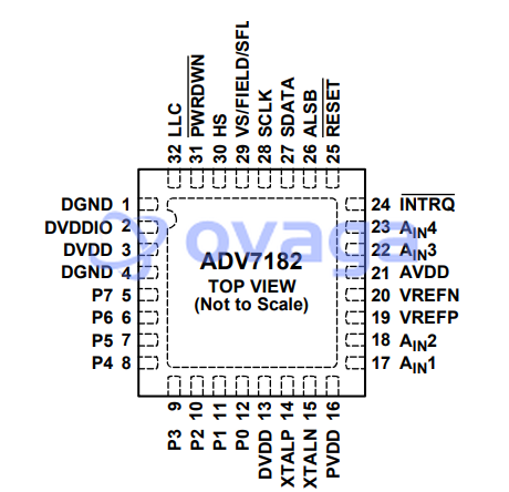
DIP (Dual In-line Package)
SOP (Small Outline Package)
QFP (Quad Flat Package)
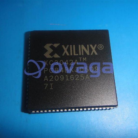
BGA (Ball Grid Array)
LGA (Land Grid Array)
CSP (Chip Scale Package)
TO (Transistor Outline)
PLCC (Plastic Leaded Chip Carrier)
QFN (Quad Flat No-Lead)
SMD (Surface Mount Device)
DIP (Dual In-line Package)
A dual in-line package (DIP) is one of the through-hole packaging types, with pins extending from both sides of the package. It is available in two materials: plastic and ceramic.
DIP is the most commonly used through-hole package and finds application in standard logic ICs, memory LSIs, microcircuits, and more. The pin pitch is 2.54mm, with pin counts ranging from 6 to 64.
The package width is typically 15.2mm. Some packages with widths of 7.52mm and 10.16mm are referred to as "skinny DIP" and "slim DIP", respectively, although in most cases, they are simply referred to as DIP. Ceramic DIP sealed with low-melting-point glass is also known as the card.
Features
-
Pins on both sides: The pins of DIP packages are arranged in a dual-column format on both sides of the package. This arrangement makes it easier to handle DIP packages during insertion into sockets or to solder onto circuit boards.
-
Suitable for larger-sized integrated circuits: DIP packages are typically used for larger-sized integrated circuit chips as they provide ample space to accommodate more pins.
-
Easy manual insertion and removal: Due to the pins of DIP packages being located on both sides of the package, they can be easily inserted or removed from sockets by hand. This facilitates convenience during chip repairs or replacements.
-
Relatively lower pin density: Compared to some modern packaging types, DIP packages have a lower pin density. This means that they may require more space in compact circuit designs.
Although DIP packages are less commonly used in modern electronic devices, they still find wide adoption in certain applications, particularly those requiring manual insertion/removal or larger-sized chips.
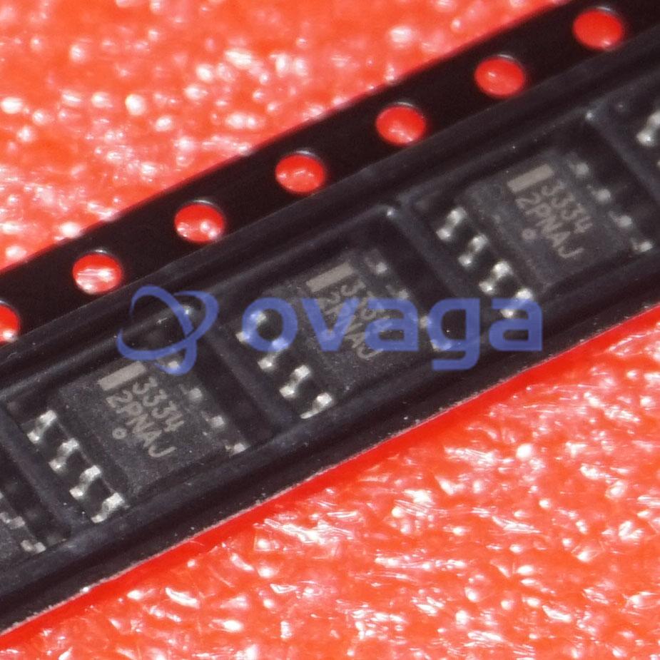
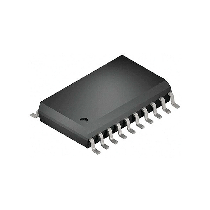
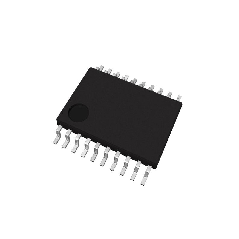
SOP (Small Outline Package)
A small outline package (SOP) is one of the surface-mount packaging types, with pins extending from both sides of the package in the shape of seagull wings (L-shape). It is available in two materials: plastic and ceramic. It is also known as Small Outline Package (SOL) or Dual Flat Package (DFP).
In addition to being used for memory LSIs, SOP is widely employed in circuits such as moderately sized Application Specific Standard Products (ASSP). In the domain of input and output terminals ranging from 10 to 40, SOP is the most commonly used surface-mount package. It has a pin pitch of 1.27mm, with a pin count ranging from 8 to 44.
Furthermore, SOP with a pin pitch smaller than 1.27mm is referred to as Small Shrink Outline Package (SSOP). SOP with an assembly height of less than 1.27mm is known as a Thin Small Outline Package (TSOP) (see SSOP, TSOP). There is also a variant of SOP that includes a heat sink.
Features
-
Compact size: SOP packaging is designed to be compact, allowing for high-density component placement within limited space. This makes it suitable for applications with restricted space.
-
Low profile: SOP packaging has a low profile, meaning it has a small vertical height above the printed circuit board (PCB). This feature is beneficial for applications with height limitations or a need for slim designs.
-
Surface mount: SOP packages utilize surface-mount technology, enabling direct soldering onto the surface of the PCB and providing reliable electrical connections. This packaging form facilitates automated production and efficient assembly processes.
SOP packaging finds extensive application in consumer electronics, communication devices, computer hardware, and other fields. It plays a vital role in miniaturization and high-performance solutions for electronic devices.
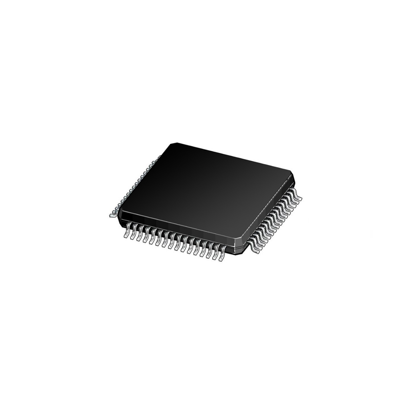
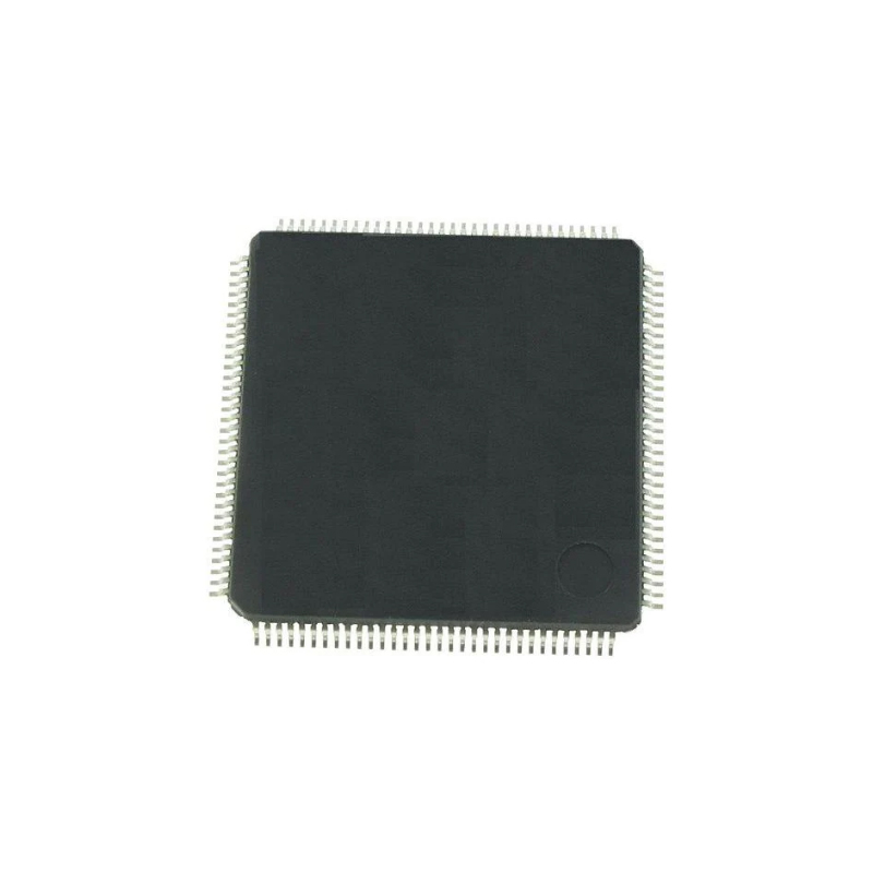
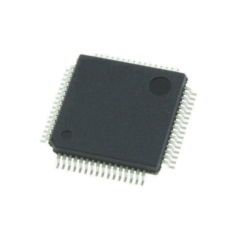
QFP (Quad Flat Package)
Quad Flat Package (QFP) is a surface-mount type of package with a flattened profile and pins extending from all four sides in a seagull-wing (L) shape. It can be fabricated using three main substrate materials: ceramic, metal, and plastic, with plastic encapsulation being the most prevalent in terms of quantity. In cases where the material is not explicitly specified, plastic QFP is commonly assumed.
Plastic QFP is the most widely used multi-pin LSI (Large Scale Integration) package. It finds application not only in digital logic LSI circuits such as microprocessors and gate arrays but also in analogue LSI circuits for VTR signal processing, audio signal processing, and similar applications.
QFP packages come in various pin pitch specifications, including 1.0mm, 0.8mm, 0.65mm, 0.5mm, 0.4mm, and 0.3mm. The 0.65mm pitch specification typically supports a maximum pin count of 304.
In Japan, QFP packages with a pin pitch smaller than 0.65mm are referred to as QFP(FP). However, the Japan Electronic and Mechanical Industries Association has recently reassessed the external specifications of QFP. Instead of distinguishing based on pin pitch, they now classify the packages into three types based on the package body thickness: QFP (2.0mm to 3.6mm thick), LQFP (1.4mm thick), and TQFP (1.0mm thick).
Additionally, some LSI manufacturers specifically designate QFP packages with a 0.5mm pin pitch as Shrink Quad Flat Package (SQFP) or VQFP.
However, some manufacturers also use the term SQFP for QFP packages with pin pitches of 0.65mm and 0.4mm, causing some degree of confusion.
One drawback of QFP packages is that when the pin pitch is less than 0.65mm, the pins are prone to bending. To mitigate pin deformation, several improved variants of QFP have been developed:
-
BQFP, which features tree-shaped buffing pads at the package corners.
-
GQFP, which includes resin protection rings covering the front end of the pins.
-
TPQFP, which incorporates test protrusions within the package body, allows testing with dedicated fixtures to prevent pin deformation.
Features
-
High pin density: QFP packages are designed to accommodate a large number of pins, making them suitable for complex circuits with numerous connections.
-
Good heat dissipation: QFP packages typically have exposed thermal pads or pins on the bottom, facilitating efficient heat dissipation for ICs that generate substantial heat during operation.
-
Convenient assembly: Due to their standardized design and flat bottom surface, QFP packages are well-suited for automated assembly processes. The pins can be easily soldered onto PCBs using surface mount technology (SMT), enabling efficient and cost-effective production.
-
Versatility: QFP packages are available in various sizes and pin configurations, offering flexibility to meet the requirements of different designs and applications. They are widely used in computer peripherals, consumer electronics, communication devices, automotive systems, and other electronic devices.
QFP packages strike a balance between pin count, space efficiency, and assembly convenience, making them highly favored in many IC applications.
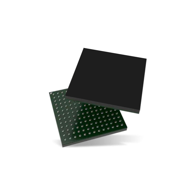
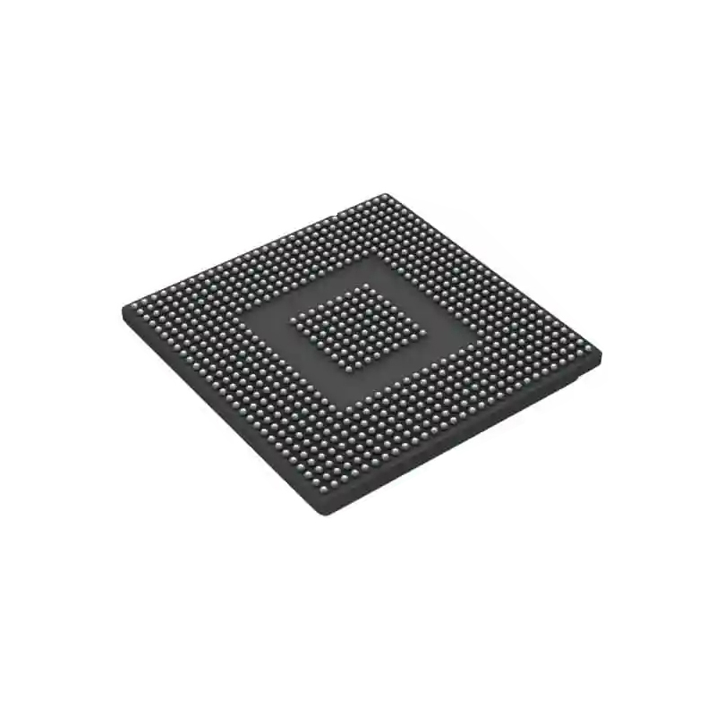
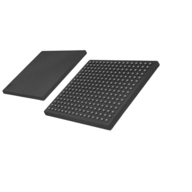
BGA (Ball Grid Array)
Ball Grid Array (BGA) is a surface-mount packaging technique that utilizes a spherical contact display. It involves the creation of spherical protrusions on the backside of a printed circuit board (PCB) to replace conventional pins. LSI chips are mounted on the front side of the PCB and then sealed using either transfer molding resin or encapsulation methods. BGA is also referred to as the Protrusion Array Carrier (PAC).
BGA is a packaging solution commonly employed in multi-pin LSIs, offering the possibility of exceeding 200 pins. The package itself can be smaller in size compared to Quad Flat Package (QFP), for instance.
For example, a 360-pin BGA with a pin pitch of 1.5mm occupies only 31mm on each side, while a 304-pin QFP with a pin pitch of 0.5mm requires 40mm on each side.
Furthermore, BGA eliminates concerns about pin deformation that are present in QFP packages.
Initially developed by Motorola in the United States, BGA was first adopted in portable telephones and other devices. It is expected to become more prevalent in personal computers in the future.
Initially, BGA had a pin pitch of 1.5mm and featured 225 pins. Presently, some LSI manufacturers are developing 500-pin BGAs.
One challenge with BGA is post-reflow appearance inspection. Effective methods for visual inspection are currently unclear.
Some argue that due to the larger pitch of the solder joints, the connections can be considered stable and can only be addressed through functional testing. Motorola refers to the resin-sealed package as OMPAC and the encapsulation-sealed package as GPAC.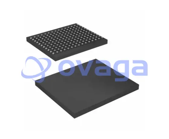
Features
-
High Density: BGA packaging accommodates a higher number of pins by arranging solder balls in a grid pattern that covers the bottom of the package. This makes BGA suitable for high-density integrated circuits, allowing for more pins in a smaller package size.
-
Excellent Electrical Performance: The reliable solder connections between the solder balls and the printed circuit board (PCB) result in low resistance and low inductance electrical connections, thereby enhancing signal transmission and electrical performance.
-
Low Inductance: The grid arrangement of solder balls reduces the transmission path between pins, minimizing inductance effects and facilitating the transmission of high-frequency signals while reducing signal noise.
-
Good Thermal Dissipation: BGA packages often incorporate bottom metal heat pads or heat balls, effectively conducting and dissipating generated heat, thereby improving the thermal dissipation performance of the integrated circuits.
-
Reliability: The grid arrangement of solder balls enhances BGA packages' resistance to mechanical stress and vibration, providing a more reliable connection and reducing issues such as pin breakage and cold soldering.
-
Versatility: BGA packages are suitable for various types of integrated circuits, including processors, FPGAs, ASICs, etc. They find wide-ranging applications in computers, communication equipment, consumer electronics, and other fields.
BGA packaging has gained popularity due to its high density, excellent electrical performance, thermal dissipation capabilities, and reliability. It has become one of the most common packaging types in modern electronic devices.
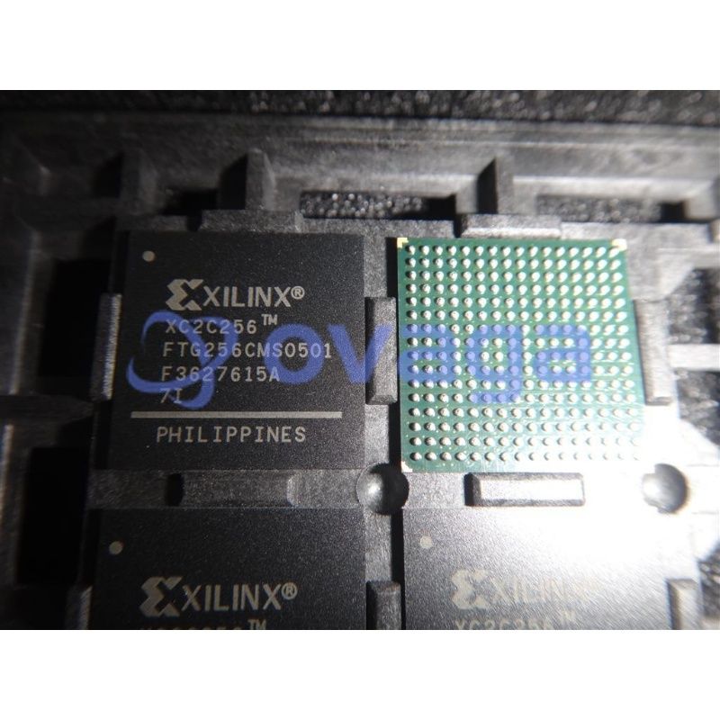
LGA (Land Grid Array)
Land Grid Array. It refers to the packaging that incorporates an array of electrode contacts on the bottom surface. It can be easily inserted into a socket during assembly. Currently, ceramic LGAs with 227 contacts (1.27mm pitch) and 447 contacts (2.54mm pitch) are being practically used in high-speed logic LSI circuits.
Compared to QFP, LGA can accommodate more input and output pins in a relatively smaller package. Additionally, its low impedance leads make it highly suitable for high-speed LSIs. However, due to the complexity and high cost involved in socket production, LGA is currently not widely used. Nevertheless, it is expected that the demand for LGA will increase in the future.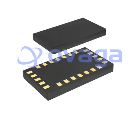
Features
-
Pad array configuration: LGA packaging employs an ordered arrangement of pads on the bottom surface. These pads provide more electrical connection points compared to traditional pin packages.
-
High-density interconnects: The design of pad arrays enables LGA packages to achieve higher pin densities, making them suitable for complex integrated circuits requiring a large number of pins.
-
Reliable electrical connections: The pads offer reliable electrical connections, ensuring stable and dependable signal transmission between the package and the PCB.
-
Thermal performance: LGA packages typically exhibit good heat dissipation characteristics. The metal contact between the pads and the PCB efficiently transfers the heat generated inside the package.
-
Wide applicability: LGA packaging finds extensive use in high-performance processors, graphics processors (GPUs), chipsets, and other integrated circuit products that demand high pin densities and efficient heat dissipation.
The key features of LGA packaging, including high pin density, reliable electrical connections, and excellent thermal performance, make it the most prevalent type of integrated circuit packaging in modern electronic devices.
CSP (Chip Scale Package)
Chip Scale Package(CSP) is characterized by its compact size, which closely matches the dimensions of the integrated circuit chip. CSP achieves high integration and miniaturization by minimizing the size of the package.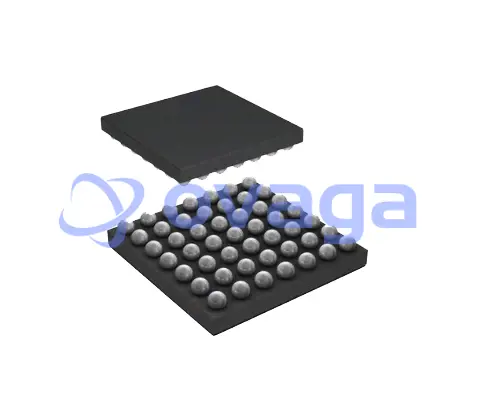
Features
-
Ultra-small size: CSP packages have extremely small dimensions, approaching those of the integrated circuit chip. This reduction in package size minimizes the space occupied, allowing for a more compact circuit layout on the circuit board, thus facilitating high-density circuit designs.
-
High integration: Due to the close proximity in size to the chip, CSP enables highly integrated circuit designs. Multiple CSP-packaged chips can accommodate more functionalities and circuit components within a smaller space.
-
Low power consumption: CSP packaging typically employs surface mount technology, which reduces power losses in signal transmission by utilizing short-distance signal transfer and tight connections between the package and the circuit board.
-
Excellent electrical performance: CSP packaging utilizes short-distance electrical connections and wiring, minimizing adverse effects such as resistance, inductance, and capacitance, thereby providing excellent electrical performance.
-
Facilitates automated production: CSP packaging is well-suited for large-scale automated production. Through advanced production equipment, efficient packaging processes can be realized, thereby enhancing production efficiency and product quality.
CSP packaging, due to its ultra-small size, high integration, low power consumption, and excellent electrical performance, finds wide application in integrated circuit products for fields such as mobile devices, wireless communications, consumer electronics, and medical devices.
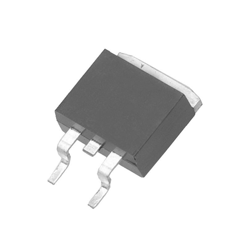
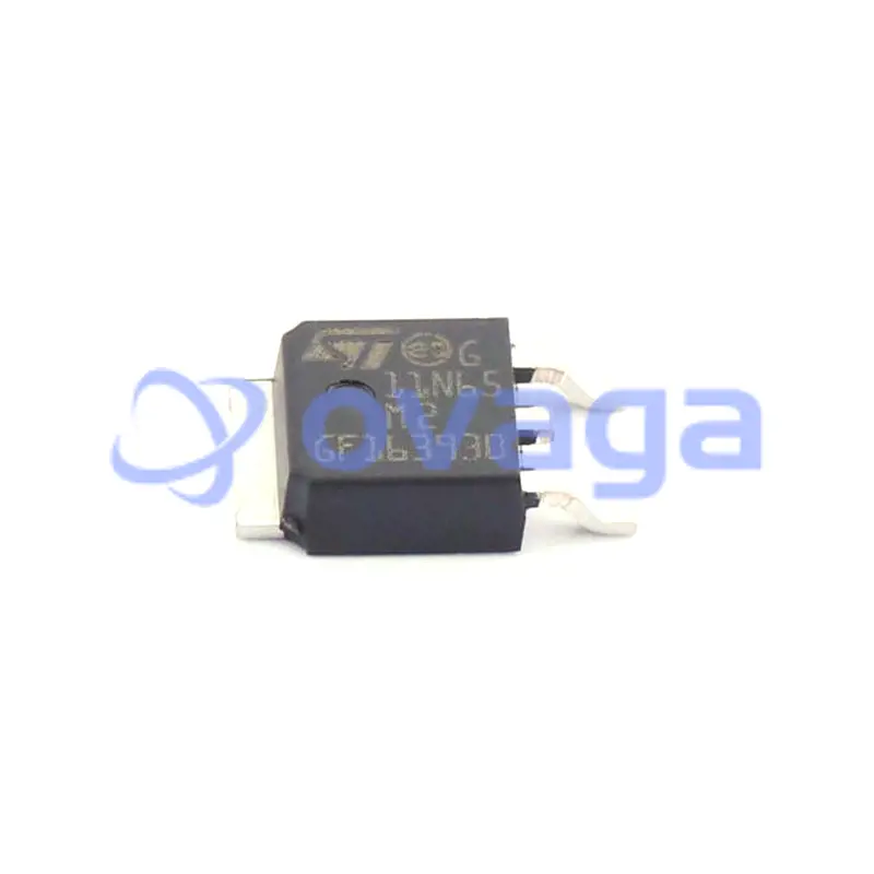
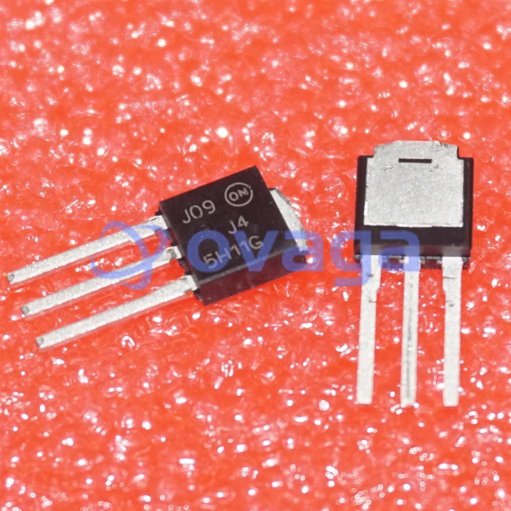
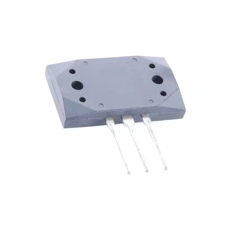
TO (Transistor Outline)
TO (Transistor Outline) is a type of transistor package primarily used for discrete transistor encapsulation. It is a standardized packaging type with a specific appearance and pin layout.
The TO package typically has a cylindrical or rectangular shape with protruding pins. It is a through-hole package and is usually connected to the circuit board through soldering or insertion.
The TO package plays a crucial role in protecting and mechanically supporting the transistor. It provides a physical barrier between the external environment and the transistor chip, safeguarding the transistor from mechanical stress, dust, moisture, and other environmental factors.
Additionally, the TO package facilitates electrical connections through the pin connections, allowing the transistor's signals and power to be extracted and enabling interaction with other circuit components or systems.
TO packages are typically numbered based on pin count and package size, such as TO-92, TO-220, etc. Each type of TO package has specific pin layouts and size specifications to accommodate different types of transistors.
They often possess certain heat-resistant properties to meet the heat dissipation requirements of high-power transistors.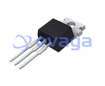
Features
-
Standardized Packaging: The TO package is a standardized packaging type with a uniform appearance and pin layout. This standardization allows TO-packaged transistors to be widely used in different circuit designs, facilitating production and usage.
-
Mechanical Support: The TO package provides mechanical support and protection for the transistor. It withstands external mechanical stress and environmental factors, enhancing the stability and reliability of the transistor.
-
Pin Connections: The TO package utilizes pin connections to extract the transistor's signals and power, enabling connection with other circuit components or systems. The pin layout and count may vary depending on the package type.
-
Heat Resistance: TO packages generally possess a certain level of heat resistance to meet the heat dissipation requirements of high-power transistors. They can operate stably within a specific temperature range and achieve heat dissipation through a pin and contact area.
-
Through-Hole Package: TO packages belong to the through-hole package type and are typically connected to the circuit board through soldering or insertion. This connection method is relatively simple, facilitating manufacturing and maintenance.
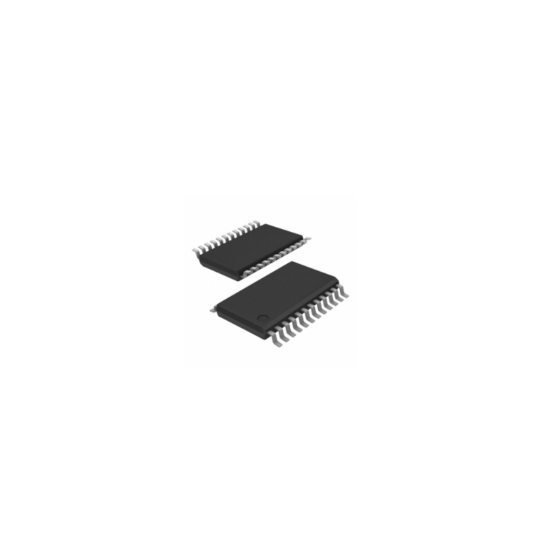
PLCC (Plastic Leaded Chip Carrier)
The Plastic Leaded Chip Carrier (PLCC) is a type of surface-mount package that serves as a chip carrier for electronic components. It features leads that extend from all four sides of the package, forming a cruciform shape. The package itself is made of plastic.
Initially introduced by Texas Instruments in 64k-bit and 256k-bit DRAMs, the PLCC has now become popular for logic LSI, DLD (or programmable logic devices), and other circuits.
The pin pitch of PLCC is 1.27mm, with pin counts ranging from 18 to 84. Its J-shaped pins are less prone to deformation compared to Quad Flat Package (QFP), making it easier to handle. However, visual inspection after soldering can be more challenging.
PLCC is similar to LCC (also known as QFN). In the past, the main distinction was that PLCC utilized plastic while LCC employed ceramic materials. However, variations have emerged, such as ceramic J-shaped pin packages and pinless plastic packages (referred to as Plastic LCC, PC LP, P-LCC, etc.), making it difficult to differentiate between the two.
To address this, the Japan Electronic Machinery Industry Association decided in 1988 to refer to the package with J-shaped pins extending from all four sides as QFJ and the package with electrode bumps on all four sides as QFN.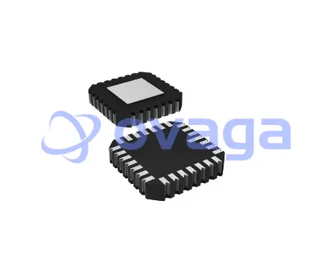
Features
-
Leaded Package: PLCC employs a leaded package design featuring multiple pins arranged around the periphery of the package. The number and arrangement of pins may vary depending on the specific package specifications.
-
Plastic Material: The PLCC package is made of plastic material, typically thermoplastic. This material offers excellent insulation properties, lightweight construction, low cost, and ease of manufacturing and processing.
-
Inverted Package: The chip in a PLCC package is typically positioned inside the package and connected to the exterior via leads. This design provides improved electrical connectivity and mechanical support while reducing the risk of chip damage during installation.
-
Thermal Dissipation: PLCC packages generally exhibit good thermal dissipation properties, effectively transferring heat generated by the chip to the exterior of the package, thereby maintaining stable operating temperatures for the chip.
-
Removability: PLCC packages can usually be detached from the chip carrier through methods like hot air reflow or other techniques, facilitating chip replacement or repair when needed.
-
Widespread Application: Due to its reliability, ease of use, and cost-effectiveness, PLCC packaging finds extensive application in various electronic devices, including computers, communication equipment, and consumer electronics.
PLCC packaging encompasses features such as leaded design, plastic material construction, inverted packaging, good thermal dissipation, removability, and wide-ranging applications. These characteristics make PLCC a common and dependable chip package suitable for diverse electronic applications.
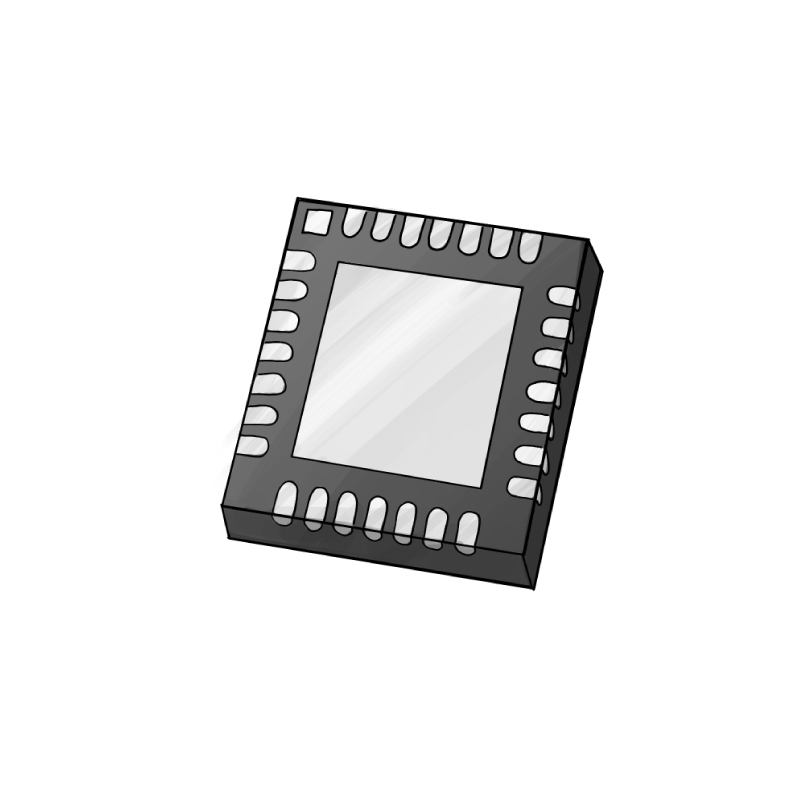
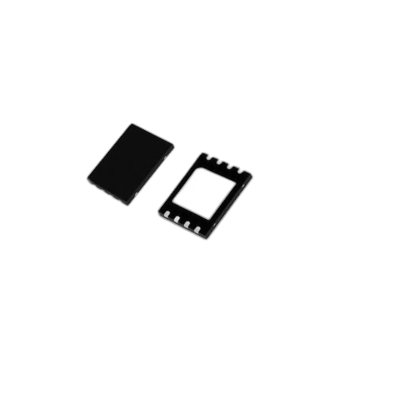
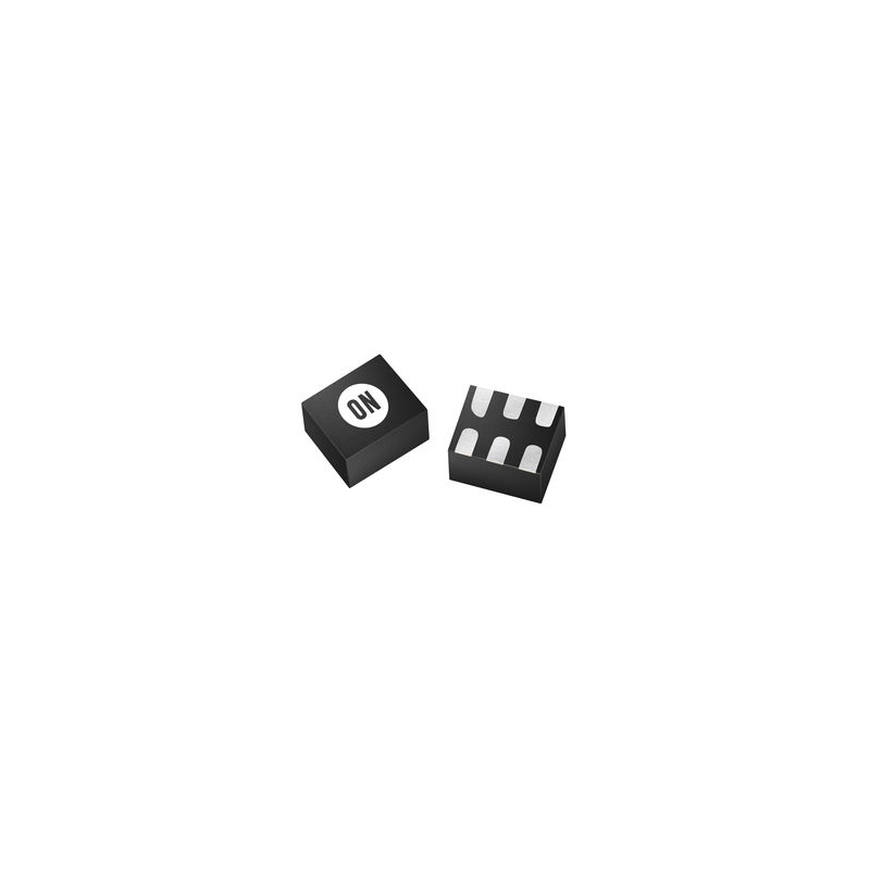
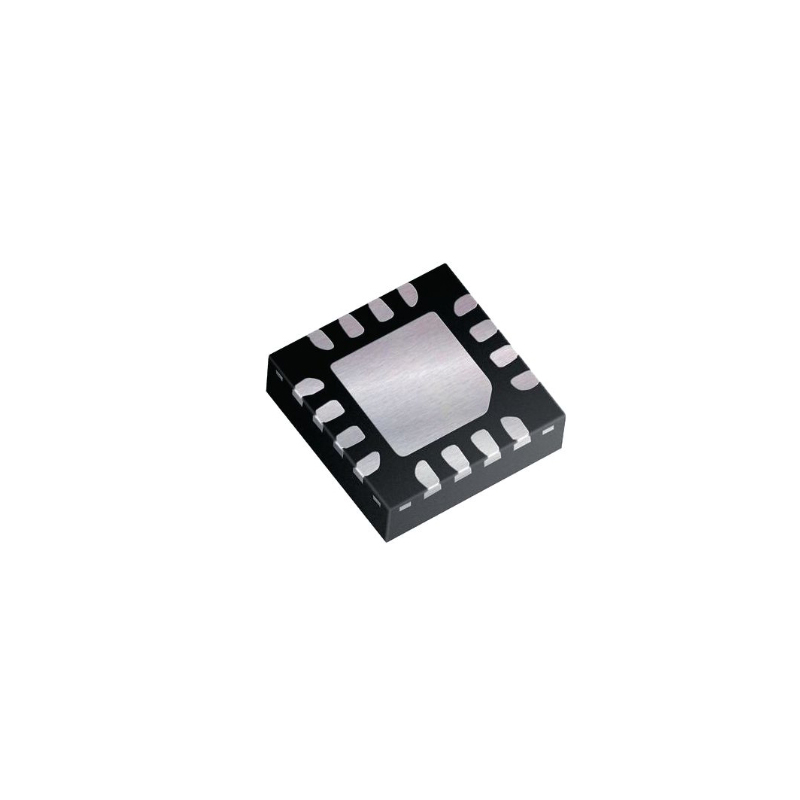
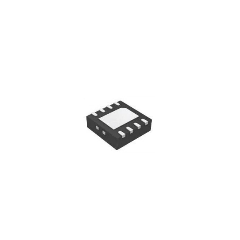
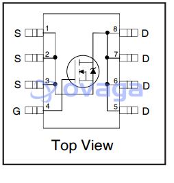
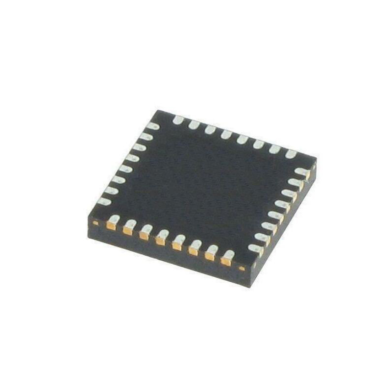
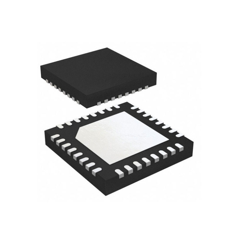
QFN (Quad Flat No-Lead)
Quad Flat No-Lead (QFN) is a type of surface-mount package and is also commonly referred to as LCC (Leadless Chip Carrier). The term QFN is defined by the Japan Electronic and Mechanical Industries Association.
The package features electrode contact points on all four sides and does not have external leads. Compared to Quad Flat Package (QFP), QFN occupies a smaller surface area and has a lower height. However, the lack of leads in QFN makes it challenging to alleviate stress between the printed circuit board and the package at the points of the electrode contact.
As a result, the electrode contact points in QFN are generally fewer in number compared to the pins in QFP, typically ranging from around 14 to 100. There are two material options: ceramic and plastic. When labeled as LCC, it usually refers to ceramic QFN. The center-to-center spacing of the electrode contact points is 1.27mm.
Plastic QFN is a cost-effective package that uses glass epoxy resin as the substrate for the printed circuit board. In addition to the 1.27mm center-to-center spacing, there are also two other options: 0.65mm and 0.5mm. This package is also known as plastic LCC, PCLC, or P-LCC.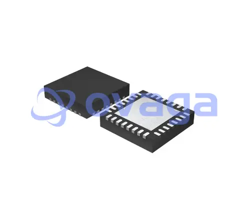
Features
-
Leadless Design: QFN packages employ a leadless design, with the pins typically located on the bottom of the package, not exposed around the package's perimeter. This design helps save space and increase package integration.
-
Package Shape: QFN packages are usually square or rectangular, with typically flat edges. The dimensions can be adjusted according to specific requirements to accommodate different chip sizes and pin counts.
-
Pad Connection: QFN packages use pads for connection to the circuit board. The pads are usually located on the bottom of the package and are connected to the circuit board's pads through soldering techniques such as solder balls or solder paste. This enables electrical connection and mechanical support.
-
Low Delay and Low Inductance: Due to the direct connection of the QFN package's pads to the metal pads on the circuit board, it exhibits lower inductance and delay, which benefits high-frequency signal performance and circuit response speed.
-
Heat Dissipation: QFN packages typically offer good heat dissipation capabilities. The pads on the package's bottom can serve as heat-conducting surfaces, effectively transferring heat generated by the chip to the circuit board or heat dissipation system, enhancing the chip's thermal management.
-
Compact Size: With the leadless design, QFN packages have smaller dimensions compared to traditional leaded packages, facilitating compact circuit board layouts and high-density integration.
-
High Reliability: QFN packages achieve stable electrical and mechanical connections through pad connections, providing reliable packaging and protection. They can maintain chip performance and stability even in harsh operating environments.
QFN packages possess characteristics such as leadless design, square or rectangular shape, pad connections, low delay and inductance, good heat dissipation, compact size, and high reliability.
These features make QFN a common and suitable chip package for various application fields, including communication equipment, consumer electronics, automotive electronics, and more.
SMD (Surface Mount Device)
SMD (Surface Mount Device) is a type of surface-mount component, also known as a surface-mount element. Unlike traditional through-hole components, the pins of SMD devices are directly soldered onto the surface of a printed circuit board (PCB) without the need for insertion through holes.
The pins of SMD devices are typically flat, small metal pads or spherical solder balls, which are soldered to corresponding pads on the PCB, achieving electrical connections and mechanical fixation. This surface-mount design makes component installation more convenient, fast, and automated, thereby enhancing production efficiency and reliability.
Features
-
Compact Size: SMD devices are smaller in size compared to traditional through-hole devices, enabling high integration and compact circuit design. This is particularly important for electronic devices that require miniaturization.
-
High Integration: Due to the surface-mount technology employed in SMD devices, more functionality and components can be integrated within relatively small spaces, providing higher integration and performance.
-
Lightweight: The small size and lightweight materials of SMD devices contribute to overall low weight, catering to the demands of slimness and portability.
-
Low Power Consumption: SMD devices typically utilize advanced semiconductor manufacturing processes, exhibiting low power consumption characteristics that contribute to improved energy efficiency and battery life.
-
High-Frequency Characteristics: SMD devices possess excellent high-frequency characteristics, making them suitable for high-frequency signal processing and communication applications.
-
Automated Production: The surface-mount nature of SMD devices lends itself to automated production processes, enabling high-speed and high-precision assembly processes, thereby improving production efficiency and quality control.
-
Reliability: With robust soldered connections to the PCB, SMD devices exhibit high mechanical strength and reliability, capable of withstanding environmental factors such as vibration, impact, and temperature variations.
Types of IC Packages - ALL
Please find below a list of IC package types and their characteristics for your reference:
BGA (Ball Grid Array)
- Pins arranged in a grid of solder balls on the package bottom, providing high pin density and connectivity
- Suitable for high-speed and high-density applications with good thermal dissipation
BQFP (Quad Flat Package with Bumper)
- Flat package with additional bumpers on the corners for improved durability and protection
C-PGA (Ceramic Pin Grid Array)
- Ceramic package with pins arranged in a grid for enhanced mechanical strength and electrical performance
C- (Ceramic)
- Ceramic package providing excellent thermal properties and high reliability
Cerdip
- Ceramic Dual Inline Package with pins extending from the bottom of the package
Cerquad
- Ceramic Quad Flat Package with pins extending from all four sides
CLCC (Ceramic Leaded Chip Carrier)
- Ceramic package with metal leads for improved electrical performance and reliability
COB (Chip on Board)
- Integrated circuit directly mounted on a PCB substrate, reducing package size and improving electrical performance
DFP (Dual Flat Package)
- Flat package with pins on two opposite sides, suitable for space-constrained applications
DIL (Dual In-Line)
- Package with pins on two parallel sides, commonly used for through-hole mounting
DIP (Dual In-Line Package)
- Classic through-hole package with pins on two parallel sides
DSO (Dual Small Outline)
- Compact package with pins on two adjacent sides, ideal for space-limited applications
DICP (Dual Inline Ceramic Package)
- Ceramic package with pins on two parallel sides, providing excellent thermal and electrical properties
DTC (Dual Tape Carrier Package)
- Package with pins extending from a tape carrier, facilitating automated assembly and handling
FP (Flat Package)
- Flat package with pins extending from the sides or bottom, suitable for low-profile applications
Flip-Chip
- Integrated circuit flipped and directly bonded to the substrate, allowing for high pin density and shorter interconnects
FQFP (Fine Pitch Quad Flat Package)
- Quad flat package with reduced pin pitch for increased pin density and improved electrical performance
CPAC (Globe Top Pad Array Carrier)
- Package with a dome-shaped top surface and an array of pads for high-density interconnections
CQFP (Quad Flat Package with Guard Ring)
- Quad flat package with an additional guard ring for improved electromagnetic compatibility and thermal dissipation
H- (with heat sink)
- Package designed with a built-in heat sink or thermal management features for improved heat dissipation
Pin Grid Array (Surface Mount Type)
- Pins arranged in a grid pattern for surface mount applications, providing high pin density and compact size
JLCC (J-Leaded Chip Carrier)
- Package with J-shaped leads for surface mount applications, offering improved electrical performance
LCC (Leadless Chip Carrier)
- Package without external leads, allowing for high-density integration and reduced package size
LGA (Land Grid Array)
- Pins arranged in a grid pattern on the package bottom, offering high pin density and reliable electrical connections
LOC (Lead on Chip)
- Package with leads directly bonded to the chip, reducing parasitic inductance and enabling high-frequency applications
LQFP (Low Profile Quad Flat Package)
- Quad flat package with reduced height for space-constrained applications
L-QUAD
- Package with leads extending from all four sides, allowing for easy assembly and electrical connections
MCM (Multi-Chip Module)
- Package incorporating multiple integrated circuits within a single module, enabling high integration levels
MFP (Mini Flat Package)
- Compact flat package with small dimensions, suitable for miniaturized applications
MQFP (Metric Quad Flat Package)
- Quad flat package with metric pitch for increased pin density and efficient PCB layout
MQUAD (Metal Quad)
- Package with metal leads extending from all four sides, providing enhanced mechanical and electrical properties
MSP (Mini Square Package)
- Small square-shaped package with leads extending from the sides, suitable for space-limited applications
OPMAC (Over Molded Pad Array Carrier)
- Package with a protective overmold and pad array for robustness and easy integration
P- (Plastic)
- Plastic package providing cost-effective and lightweight solutions for a wide range of applications
PAC (Pad Array Carrier)
- Package with an array of pads for high-density interconnections, facilitating advanced packaging techniques
PCLP (Printed Circuit Board Leadless Package)
- Leadless package directly mounted on a PCB for enhanced electrical performance and miniaturization
PFPF (Plastic Flat Package)
- Flat package with plastic body and leads extending from the sides, offering versatility and ease of handling
PGA (Pin Grid Array)
- Pins arranged in a grid pattern for through-hole mounting, providing reliable electrical connections
Piggy Back
- Package mounted on top of another package, enabling stacked configurations and increased functionality
PLCC (Plastic Leaded Chip Carrier)
- Plastic package with metal leads for improved electrical performance and ease of assembly
P-LCC (Plastic Leaded Chip Carrier)
- Plastic package without external leads, offering high-density integration and reduced package size
QFH (Quad Flat High Package)
- Quad flat package with increased height for accommodating taller components
QFI (Quad Flat I-Leaded Package)
- Quad flat package with I-shaped leads, providing enhanced mechanical strength and electrical performance
QFJ (Quad Flat J-Leaded Package)
- Quad flat package with J-shaped leads for improved electrical performance and heat dissipation
QFN (Quad Flat No-Lead Package)
- Package with no leads extending from the sides, allowing for high pin density, compact size, and improved electrical performance
QFP (Quad Flat Package)
- Flat package with pins extending from the sides, suitable for a wide range of applications
QFP (FP) (QFP Fine Pitch)
- Quad flat package with fine pitch for increased pin density and improved electrical performance
QIC (Quad In-Line Ceramic Package)
- Ceramic package with pins on four sides, offering excellent thermal properties and electrical performance
QIP (Quad In-Line Plastic Package)
- Plastic package with pins on four sides, providing cost-effective and versatile solutions
QTCP (Quad Tape Carrier Package)
- Package with a tape carrier for high-density interconnections, offering efficient assembly and handling
QTP (Quad Tape Carrier Package)
- Package with a quad tape carrier for compact size and ease of integration
QUIL (Quad In-Line)
- Package with leads extending from all four sides, providing ease of assembly and electrical connections
QUIP (Quad In-Line Package)
- Package with leads extending from all four sides for improved electrical performance and heat dissipation
SDIP (Shrink Dual In-Line Package)
- Dual in-line package with reduced size for space-constrained applications
SH-DIP (Shrink Dual In-Line Package)
- Dual in-line package with shrink size and improved electrical performance
SIL (Single In-Line)
- Package with a single row of leads, suitable for low-pin count applications
SIMM (Single In-Line Memory Module)
- Package for memory modules with a single row of leads, enabling memory integration
SIP (Single In-Line Package)
- Package with a single row of leads for compact size and easy integration
SK-DIP (Skinny Dual In-Line Package)
- Dual in-line package with a slim profile for space-saving applications
SL-DIP (Slim Dual In-Line Package)
- Dual in-line package with a slim profile for space-efficient assembly
SMD (Surface Mount Devices)
- Devices designed for surface mount applications, offering space-saving, automated assembly capabilities
SO (Small Outline)
- Package with a small and compact outline for space-constrained applications
SOI (Small Outline I-Leaded Package)
- Small outline package with I-shaped leads, providing improved mechanical strength and electrical performance
SOIC (Small Outline Integrated Circuit)
- Small outline package for integrated circuits, offering space-saving and reliable electrical connections
SOJ (Small Outline J-Leaded Package)
- Small outline package with J-shaped leads, providing enhanced electrical performance and heat dissipation
SQL (Small Outline L-Leaded Package)
- Small outline package with L-shaped leads, offering improved electrical performance and ease of assembly
SONF (Small Outline Non-Fin)
- Small outline package without fins, suitable for compact and low-profile applications
SOF (Small Outline Package)
- Small outline package with compact size and versatile applications
SOW (Small Outline Package - Wide Type)
- Small outline package with wider dimensions for enhanced electrical performance and heat dissipation
COB (Chip On Board)
- Package where the IC chip is directly mounted onto a PCB, providing compact integration and cost-effectiveness
COG (Chip on Glass)
- Package where the IC chip is mounted directly on a glass substrate, offering high-density integration and compact size
Conclusion
With the maturity of chip technology and the rapid improvement of chip yield, the cost of back-end packaging has become increasingly significant in the overall integrated circuit cost. The ever-changing and rapidly developing packaging technologies are overwhelming.
It is our hope that this article will provide you with valuable insights, enabling you to gain a deeper understanding of integrated circuit packaging.
Read More:
Small Outline Integrated Circuit - SOIC
IC Package Types and Their Features
Small Outline Package (SOP): Definition, Applications and Advantages
Extended Reading
 FAQ
FAQ
-
What are the advantages of Ball Grid Array (BGA) packages?
BGA packages offer improved electrical performance, higher pin counts, better thermal dissipation, and increased reliability compared to other package types. They are commonly used in applications requiring high-density and high-speed components.
-
What is the difference between Through-Hole and Surface Mount packages?
Through-Hole packages have leads that pass through holes on the PCB and are soldered on the opposite side, while Surface Mount packages have no leads and are directly mounted on the surface of the PCB.
-
What factors should be considered when selecting an IC package type?
When choosing an IC package type, factors such as cost, size, thermal performance, electrical characteristics, and reliability requirements should be considered.
Popular Blogs
-
Small Outline Packag...
SOP (Small Outline Package) is a type of integra...
-
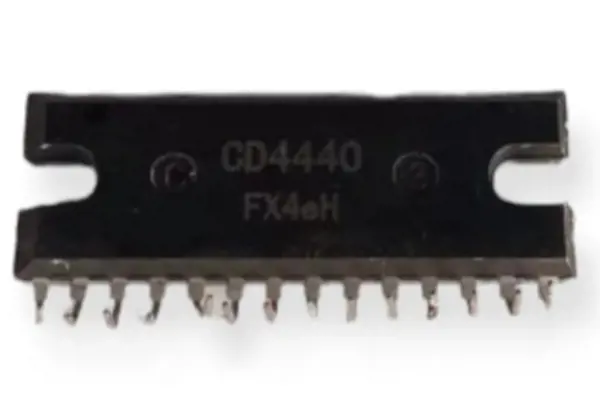
CD4440 IC: Datasheet...
The CD4440 IC is a stereo audio power amplifier ...
-

Advantages and Disad...
Operational amplifiers, or op-amps, offer a host...
-
Dual Inline Package ...
Dual in-line package, also known as DIP package ...
Hot Products
-
-
-
-
-
-
-
-
-
-

-
-
-
-
-
-
-
-
-
-
-
-
-
-
-
-
-
-
Infineon Technologies Corporation
100V Single N-Channel HEXFET Power MOSFET in a PQF...
-
Infineon Technologies Corporation
100V Single N-Channel HEXFET Power MOSFET in a D2-...
-
Infineon Technologies Corporation
150V Single N-Channel HEXFET Power MOSFET in a 5mm...
-
Infineon Technologies Corporation
150V Single N-Channel HEXFET Power MOSFET in a D2-...
-
Infineon Technologies Corporation
200V Single N-Channel HEXFET Power MOSFET in a D2-...
-
-
Infineon Technologies Corporation
250V Single N-Channel HEXFET Power MOSFET PDP Swit...
-
-
-
-
-
Infineon Technologies Corporation
60V Single N-Channel HEXFET Power MOSFET in a PQFN...
-
Infineon Technologies Corporation
A 30V Single N-Channel HEXFET Power MOSFET in a Di...
-
-
-
-
-
-
-
-
-
-
Popular Manufacturers