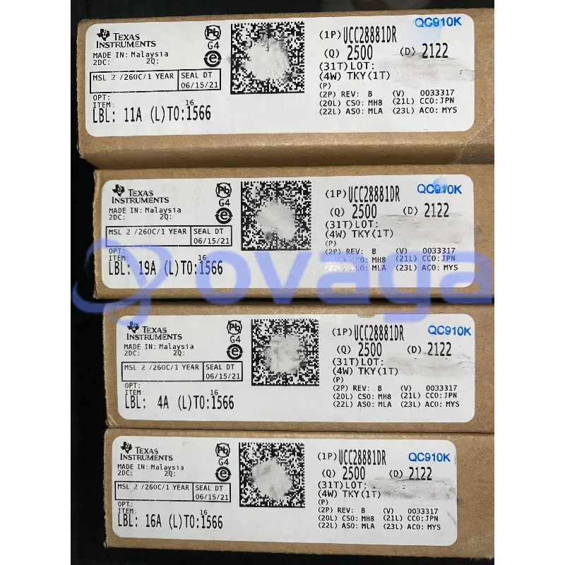
Images are for reference only See Product Specifications
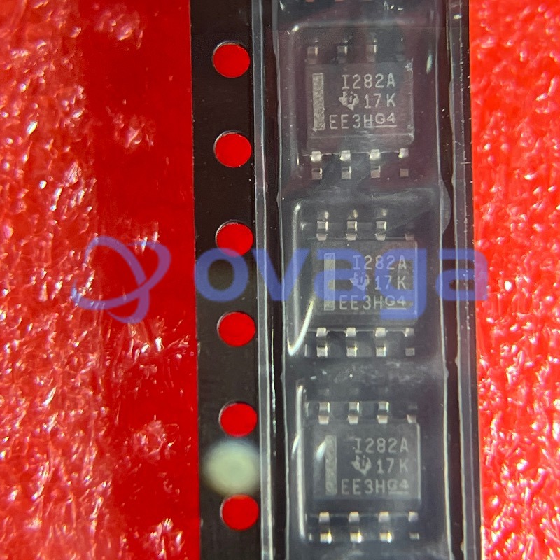
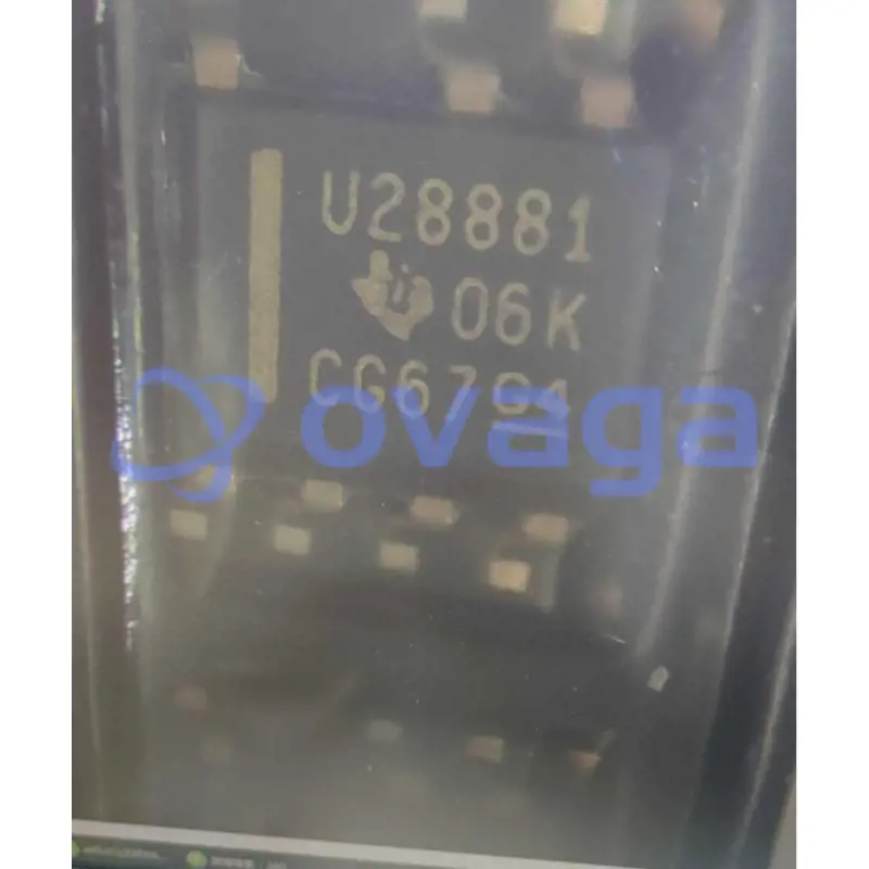
TI UCC27524DSDR
Low-Side Gate Driver IC Non-Inverting 8-SON (3x3)


Brands: TI
Mfr.Part #: UCC27524DSDR
Datasheet: UCC27524DSDR Datasheet (PDF)
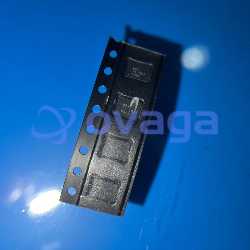
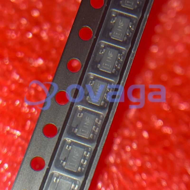
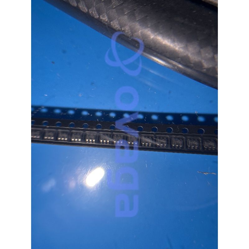
Package/Case: SON-8
RoHS Status:
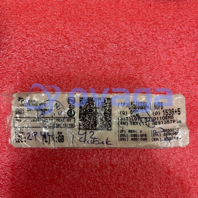
Stock Condition: 15000 pcs, New Original
Product Type: Power Driver ICs
0
1
*All prices are in USD
| Qty | Unit Price | Ext Price |
|---|---|---|
| 1 | $0.687 | $0.687 |
| 10 | $0.593 | $5.930 |
| 30 | $0.540 | $16.200 |
| 100 | $0.481 | $48.100 |
| 500 | $0.373 | $186.500 |
| 1000 | $0.363 | $363.000 |
In Stock:15000 PCS
UCC27524DSDR General Description
The UCC2752x family of devices are dual-channel, high-speed, low-side gate-driver devices capable of effectively driving MOSFET and IGBT power switches. Using a design that inherently minimizes shoot-through current, UCC2752x can deliver high-peak current pulses of up to 5-A source and 5-A sink into capacitive loads along with rail-to-rail drive capability and extremely small propagation delay (typically 13 ns). In addition, the drivers feature matched internal propagation delays between the two channels. These delays are very well suited for applications requiring dual-gate drives with critical timing, such as synchronous rectifiers. This also enables connecting two channels in parallel to effectively increase current-drive capability or driving two switches in parallel with one input signal. The input pin thresholds are based on TTL and CMOS compatible low-voltage logic, which is fixed and independent of the VDD supply voltage. Wide hysteresis between the high and low thresholds offers excellent noise immunity.
The UCC2752x family provide the combination of three standard logic options dual inverting, dual noninverting, one inverting and one noninverting driver. UCC27526 features a dual input design which offers flexibility of both inverting (IN pin) and non-inverting (IN+ pin) configuration for each channel. Either IN+ or IN pin controls the state of the driver output. The unused input pin is used for enable and disable functions. For safety purpose, internal pullup and pulldown resistors on the input pins of all the devices in UCC2752x family ensure that outputs are held LOW when input pins are in floating condition. The UCC27523, UCC27524, and UCC27525 devices feature Enable pins (ENA and ENB) to have better control of the operation of the driver applications. The pins are internally pulled up to VDD for active-high logic and are left open for standard operation.
UCC2752x family of devices are available in SOIC-8 (D), MSOP-8 with exposed pad (DGN) and 3-mm × 3-mm WSON-8 with exposed pad (DSD) packages. UCC27524 is also offered in PDIP-8 (P) package. UCC27526 is only offered in 3-mm × 3-mm WSON (DSD) package.
Features
- Industry-Standard Pinout
- Two Independent Gate-Drive Channels
- 5-A Peak Source and Sink-Drive Current
- Independent-Enable Function for Each Output
- TTL and CMOS Compatible Logic Threshold
Independent of Supply Voltage - Hysteretic-Logic Thresholds for High Noise
Immunity - Inputs and Enable Pin-Voltage Levels Not
Restricted by VDD Pin Bias Supply Voltage - 4.5-V to 18-V Single-Supply Range
- Outputs Held Low During VDD-UVLO, (Ensures
Glitch-Free Operation at Power up and Power
Down) - Fast Propagation Delays (13-ns Typical)
- Fast Rise and Fall Times (7-ns and 6-ns Typical)
- 1-ns Typical Delay Matching Between Two
Channels - Two Outputs are in Parallel for Higher Drive
Current - Outputs Held Low When Inputs Floating
- PDIP (8), SOIC (8), MSOP (8) PowerPAD™ and
3-mm × 3-mm WSON-8 Package Options - Operating Temperature Range of –40°C to 140°C
Specifications
| Parameter | Value | Parameter | Value |
|---|---|---|---|
| Number of channels | 2 | Power switch | GaNFET, IGBT, MOSFET |
| Peak output current (A) | 5 | Input VCC (min) (V) | 4.5 |
| Input VCC (max) (V) | 18 | Features | Enable pin |
| Operating temperature range (°C) | -40 to 140 | Rise time (ns) | 7 |
| Fall time (ns) | 6 | Propagation delay time (µs) | 0.013 |
| Input threshold | CMOS, TTL | Channel input logic | Dual, Non-Inverting |
| Input negative voltage (V) | 0 | Rating | Catalog |
| Undervoltage lockout (typ) (V) | 4 |
Shipping
| Shipping Type | Ship Fee | Lead Time | |
|---|---|---|---|
 |
DHL | $20.00-$40.00 (0.50 KG) | 2-5 days |
 |
Fedex | $20.00-$40.00 (0.50 KG) | 2-5 days |
 |
UPS | $20.00-$40.00 (0.50 KG) | 2-5 days |
 |
TNT | $20.00-$40.00 (0.50 KG) | 2-5 days |
 |
EMS | $20.00-$40.00 (0.50 KG) | 2-5 days |
 |
REGISTERED AIR MAIL | $20.00-$40.00 (0.50 KG) | 2-5 days |
Processing Time:Shipping fee depend on different zone and country.
Payment
| Terms of payment | Hand Fee | |
|---|---|---|
 |
Wire Transfer | charge US$30.00 banking fee. |
 |
Paypal | charge 4.0% service fee. |
 |
Credit Card | charge 3.5% service fee. |
 |
Western Union | charge US.00 banking fee. |
 |
Money Gram | charge US$0.00 banking fee. |
Guarantees
1.The electronic components you purchase include 365 Days Warranty, We guarantee product quality.
2.If some of the items you received aren't of perfect quality, we would resiponsibly arrange your refund or replacement. But the items must remain their orginal condition.
Packing
-

Step1 :Product
-

Step2 :Vacuum packaging
-

Step3 :Anti-static bag
-

Step4 :Individual packaging
-

Step5 :Packaging boxes
-

Step6 :bar-code shipping tag
All the products will packing in anti-staticbag. Ship with ESD antistatic protection.
Outside ESD packing’s lable will use ourcompany’s information: Part Mumber, Brand and Quantity.
We will inspect all the goods before shipment,ensure all the products at good condition and ensure the parts are new originalmatch datasheet.
After all the goods are ensure no problems afterpacking, we will packing safely and send by global express. It exhibitsexcellent puncture and tear resistance along with good seal integrity.


Part points
-
The UCC27524DSDR is a dual-channel gate driver chip designed for controlling power MOSFETs and IGBTs in high-frequency switching applications. It features a high peak output current, fast rise and fall times, and an advanced protection and fault-reporting system. This chip is commonly used in motor drives, solar inverters, and other power electronics systems.
-
Equivalent
Equivalent products of UCC27524DSDR chip include UCC27524ADR, UCC27524DR, and UCC27524NSR. These chips are dual-channel, low-side gate driver ICs designed for driving N-channel power MOSFETs or IGBTs in high-side or low-side configurations, with features such as fast switching speed and adjustable output rise and fall times. -
Features
The UCC27524DSDR is a high-speed, dual-channel gate driver with 5-A peak sink and source current capability per channel. It features an input voltage range of 4.5 V to 18 V, integrated negative voltage regulator, and matched internal propagation delays for both channels. It also has an integrated dead time of 70 ns. -
Pinout
The UCC27524DSDR is a dual-channel, high-speed gate driver with a 14-pin count. It is designed to drive MOSFETs or IGBTs in high-power applications such as motor control and power inverters. Each channel features an independent inputs and outputs for optimal control and protection of power devices. -
Manufacturer
The manufacturer of the UCC27524DSDR is Texas Instruments. Texas Instruments is a global semiconductor design and manufacturing company that develops analog and embedded processing chips for various applications, including automotive, industrial, and consumer electronics. -
Application Field
The UCC27524DSDR is commonly used in applications such as motor drives, power inverters, and high power switching applications. It is designed to provide robust and high-speed gate drive for power MOSFETs and IGBTs, making it suitable for a wide range of high-power, high-voltage applications. -
Package
The UCC27524DSDR chip is in a surface-mount DSBGA package. It comes in a form of a dual-channel gate driver with an exposed pad for better thermal performance. The size of the package is 4 mm x 4 mm.
We provide high quality products, thoughtful service and after sale guarantee
-

We have rich products, can meet your various needs.
-

Minimum order quantity starts from 1pcs.
-

Lowest international shipping fee starts from $0.00
-

365 days quality guarantee for all products