Images are for reference only See Product Specifications
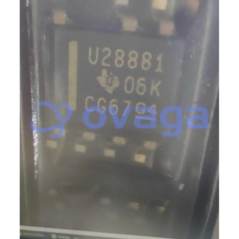
TI UCC20520DWR
5.7-kVrms, 4-A/6-A dual-channel isolated gate driver with single input, 8-V UVLO & LGA package


Brands: Texas Instruments
Mfr.Part #: UCC20520DWR
Datasheet: UCC20520DWR Datasheet (PDF)
Package/Case: 16-SOIC
Product Type: Galvanically Isolated Gate Drivers
UCC20520DWR General Description
The UCC20520 is an isolated single input, dual-channel gate driver with 4-A source and 6-A sink peak current. It is designed to drive power MOSFETs, IGBTs, and SiC MOSFETs up to 5-MHz with best-in-class propagation delay and pulse-width distortion.
The input side is isolated from the two output drivers by a 5.7-kVRMS reinforced isolation barrier, with a minimum of 100-V/ns common-mode transient immunity (CMTI). Internal functional isolation between the two secondary-side drivers allows a working voltage of up to 1500-VDC.
This driver can be used for half-bridge driver with programmable dead time (DT). A disable pin shuts down both outputs simultaneously when it is set high, and allows normal operation when left open or grounded. As a fail-safe measure, primary-side logic failures force both outputs low.
The device accepts VDD supply voltages up to 25-V. A wide input VCCI range from 3-V to 18-V makes the driver suitable for interfacing with both analog and digital controllers. All the supply voltage pins have under voltage lock-out (UVLO) protection.
With all these advanced features, the UCC20520 enables high efficiency, high power density, and robustness in a wide variety of power applications.
Features
- Single input, dual output
- Operating temperature range: –40 to 125°C
- Switching parameters:
- 19-ns typical propagation delay
- 10-ns minimum pulse width
- 5-ns maximum delay matching
- 6-ns maximum pulse-width distortion
- Common-mode transient immunity (CMTI) greater than 100-V/ns
- Surge immunity up to 12.8-kV
- Isolation barrier life >40 Years
- 4-A peak source, 6-A peak sink output
- TTL and CMOS compatible inputs
- 3-V to 18-V input VCCI range to interface with both digital and analog controllers
- Up to 25-V VDD output drive supply
- Programmable dead time
- Rejects input pulses and noise transients shorter than 5-ns
- Fast disable for power sequencing
- Industry standard wide body SOIC-16 (DW) package
- Safety-related and regulatory approvals:
- 8000-VPK isolation per DIN V VDE V 0884-11:2017-01
- 5700-VRMS isolation for 1 minute per UL 1577
- CSA certification per IEC 60950-1, IEC 62368-1, IEC 61010-1 and IEC 60601-1 end equipment standards
- CQC certification per GB4943.1-2011
Specifications
| Parameter | Value | Parameter | Value |
|---|---|---|---|
| Manufacturer | Texas Instruments | Product Category | Galvanically Isolated Gate Drivers |
| RoHS | Details | Series | UCC20520 |
| Type | High-Side, Low-Side | Mounting Style | SMD/SMT |
| Package / Case | SOIC-16 | Number of Drivers | 2 Driver |
| Number of Outputs | 2 Output | Output Current | 6 A |
| Supply Voltage - Min | 3 V | Supply Voltage - Max | 18 V |
| Rise Time | 6 ns | Fall Time | 7 ns |
| Minimum Operating Temperature | - 40 C | Maximum Operating Temperature | + 125 C |
| Technology | Si | Brand | Texas Instruments |
| Development Kit | UCC20520EVM-286 | Moisture Sensitive | Yes |
| Operating Supply Current | 2.5 mA | Output Voltage | 9.2 V to 25 V |
| Pd - Power Dissipation | 1.05 W | Product | Isolated Gate Drivers |
| Product Type | Galvanically Isolated Gate Drivers | Propagation Delay - Max | 30 ns |
| Shutdown | No Shutdown | Factory Pack Quantity | 2000 |
| Subcategory | PMIC - Power Management ICs | Unit Weight | 0.026293 oz |
| Number of channels | 2 | Isolation rating | Reinforced |
| Withstand isolation voltage (VISO) (Vrms) | 5700 | Working isolation voltage (VIOWM) (Vrms) | 2121 |
| Transient isolation voltage (VIOTM) (VPK) | 8000 | Power switch | IGBT, MOSFET, SiCFET |
| Peak output current (A) | 6 | Features | Disable, Programmable dead time |
| Output VCC/VDD (max) (V) | 25 | Output VCC/VDD (min) (V) | 9.2 |
| Input VCC (min) (V) | 3 | Input VCC (max) (V) | 18 |
| Propagation delay time (µs) | 0.019 | Input threshold | CMOS, TTL |
| Operating temperature range (°C) | -40 to 125 | Rating | Catalog |
| Bus voltage (max) (V) | 2121 | Rise time (ns) | 6 |
| Fall time (ns) | 7 |
Shipping
| Shipping Type | Ship Fee | Lead Time | |
|---|---|---|---|
 |
DHL | $20.00-$40.00 (0.50 KG) | 2-5 days |
 |
Fedex | $20.00-$40.00 (0.50 KG) | 2-5 days |
 |
UPS | $20.00-$40.00 (0.50 KG) | 2-5 days |
 |
TNT | $20.00-$40.00 (0.50 KG) | 2-5 days |
 |
EMS | $20.00-$40.00 (0.50 KG) | 2-5 days |
 |
REGISTERED AIR MAIL | $20.00-$40.00 (0.50 KG) | 2-5 days |
Processing Time:Shipping fee depend on different zone and country.
Payment
| Terms of payment | Hand Fee | |
|---|---|---|
 |
Wire Transfer | charge US$30.00 banking fee. |
 |
Paypal | charge 4.0% service fee. |
 |
Credit Card | charge 3.5% service fee. |
 |
Western Union | charge US.00 banking fee. |
 |
Money Gram | charge US$0.00 banking fee. |
Guarantees
1.The electronic components you purchase include 365 Days Warranty, We guarantee product quality.
2.If some of the items you received aren't of perfect quality, we would resiponsibly arrange your refund or replacement. But the items must remain their orginal condition.
Packing
-

Step1 :Product
-

Step2 :Vacuum packaging
-

Step3 :Anti-static bag
-

Step4 :Individual packaging
-

Step5 :Packaging boxes
-

Step6 :bar-code shipping tag
All the products will packing in anti-staticbag. Ship with ESD antistatic protection.
Outside ESD packing’s lable will use ourcompany’s information: Part Mumber, Brand and Quantity.
We will inspect all the goods before shipment,ensure all the products at good condition and ensure the parts are new originalmatch datasheet.
After all the goods are ensure no problems afterpacking, we will packing safely and send by global express. It exhibitsexcellent puncture and tear resistance along with good seal integrity.


We provide high quality products, thoughtful service and after sale guarantee
-

We have rich products, can meet your various needs.
-

Minimum order quantity starts from 1pcs.
-

Lowest international shipping fee starts from $0.00
-

365 days quality guarantee for all products