Images are for reference only See Product Specifications
Orders Over
$5000
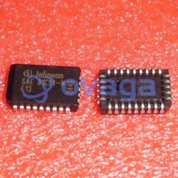
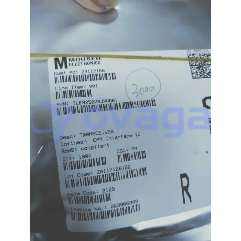
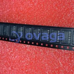
Infineon TLE9250VSJXUMA1

CAN 5Mbps 3.3V/5V Automotive AEC-Q100 8-Pin DSO T/R


Brands: Infineon Technologies Corporation
Mfr.Part #: TLE9250VSJXUMA1
Datasheet: TLE9250VSJXUMA1 Datasheet (PDF)
Package/Case: PG-DSO-8
RoHS Status:
Stock Condition: 3,700 pcs, New Original
Product Type: Drivers, Receivers, Transceivers
Warranty: 1 Year Ovaga Warranty - Find Out More
0
1
*All prices are in USD
| Qty | Unit Price | Ext Price |
|---|---|---|
| 1 | $0.895 | $0.895 |
| 10 | $0.743 | $7.430 |
| 30 | $0.667 | $20.010 |
| 100 | $0.591 | $59.100 |
| 500 | $0.546 | $273.000 |
| 1000 | $0.523 | $523.000 |
In Stock: 3,700 PCS
TLE9250VSJXUMA1 General Description
Can Fd Transceiver, Aec-Q100, 5Mbps, Soic; Ic Interface Type:Can; No. Of Tx Buffers:-; No. Of Rx Buffers:-; Supply Voltage Min:3V; Supply Voltage Max:5.5V; No. Of Pins:8Pins; Operating Temperature Min:-40°C; Operating Temperature Rohs Compliant: Yes |Infineon TLE9250VSJXUMA1
Features
- Fully compliant to ISO 11898-2 (2016)
- Guaranteed loop delay symmetry to support CAN FD data frames up to 5 MBit/s
- Very low electromagnetic emission (EME) allows the use without additional common mode choke
- VIO input for voltage adaption to the microcontroller interface (3.3V or 5V)
- Power-save mode
- Also available in tiny, leadless PG-TSON-8 package ready for automated optical inspection (AOI)
- Excellent ESD robustness
- Extended supply range on the V CC
- TxD time-out function
- Wide common mode range for electromagnetic immunity (EMI)
- Very low CAN bus leakage current in power-down state
Specifications
| Parameter | Value | Parameter | Value |
|---|---|---|---|
| RHoS | yes | PBFree | yes |
| HalogenFree | yes |
Shipping
| Shipping Type | Ship Fee | Lead Time | |
|---|---|---|---|
 |
DHL | $20.00-$40.00 (0.50 KG) | 2-5 days |
 |
Fedex | $20.00-$40.00 (0.50 KG) | 2-5 days |
 |
UPS | $20.00-$40.00 (0.50 KG) | 2-5 days |
 |
TNT | $20.00-$40.00 (0.50 KG) | 2-5 days |
 |
EMS | $20.00-$40.00 (0.50 KG) | 2-5 days |
 |
REGISTERED AIR MAIL | $20.00-$40.00 (0.50 KG) | 2-5 days |
Processing Time:Shipping fee depend on different zone and country.
Payment
| Terms of payment | Hand Fee | |
|---|---|---|
 |
Wire Transfer | charge US$30.00 banking fee. |
 |
Paypal | charge 4.0% service fee. |
 |
Credit Card | charge 3.5% service fee. |
 |
Western Union | charge US.00 banking fee. |
 |
Money Gram | charge US$0.00 banking fee. |
Guarantees
1.The electronic components you purchase include 365 Days Warranty, We guarantee product quality.
2.If some of the items you received aren't of perfect quality, we would resiponsibly arrange your refund or replacement. But the items must remain their orginal condition.
Packing
-

Step1 :Product
-

Step2 :Vacuum packaging
-

Step3 :Anti-static bag
-

Step4 :Individual packaging
-

Step5 :Packaging boxes
-

Step6 :bar-code shipping tag


All the products will packing in anti-staticbag. Ship with ESD antistatic protection.
Outside ESD packing’s lable will use ourcompany’s information: Part Mumber, Brand and Quantity.
We will inspect all the goods before shipment,ensure all the products at good condition and ensure the parts are new originalmatch datasheet.
After all the goods are ensure no problems afterpacking, we will packing safely and send by global express. It exhibitsexcellent puncture and tear resistance along with good seal integrity.


Part points
-
The TLE9250VSJXUMA1 chip is a versatile automotive-grade System Basis Chip (SBC) designed for various applications in automotive electronics. It integrates a power supply system, a CAN transceiver, a LIN transceiver, and a voltage regulator into a single package. This chip provides a cost-effective and space-saving solution for automotive communication networks, enabling reliable communication between various electronic control units (ECUs) in vehicles.
-
Equivalent
Some equivalent products to the TLE9250VSJXUMA1 chip are the TJA1055T and the TJA1057GT, which are both LIN transceivers compatible with 12V automotive applications. These chips have similar features and functionalities, making them suitable alternatives for the TLE9250VSJXUMA1 chip. -
Features
The TLE9250VSJXUMA1 is a FlexRay transceiver with a low-power mode. It operates at a supply voltage range of 5V to 27V and provides a differential voltage output through an integrated high-voltage NMOS driver. It offers a temperature range of -40°C to +150°C and supports data rates up to 10Mbps. -
Pinout
The TLE9250VSJXUMA1 is an SPI-to-VAN transceiver with LIN2.2 and J2602 support. It has 20 pins and the function is to provide communication between an external microcontroller and a Local Interconnect Network (LIN) bus. -
Manufacturer
The manufacturer of the TLE9250VSJXUMA1 is Infineon Technologies. It is a multinational semiconductor company that produces various products including microcontrollers, power management ICs, sensors, and automotive electronics. -
Application Field
The TLE9250VSJXUMA1 is a highly integrated LIN transceiver designed for automotive applications. It can be used in various areas such as automotive body control modules, seat control modules, HVAC systems, power mirrors, sunroof control, and other LIN bus applications. -
Package
The TLE9250VSJXUMA1 chip is available in a small VSSOP-8 package type. It has a form factor of JX and a compact size suitable for various applications.


Datasheet PDF
We provide high quality products, thoughtful service and after sale guarantee
-

We have rich products, can meet your various needs.
-

Minimum order quantity starts from 1pcs.
-

Lowest international shipping fee starts from $0.00
-

365 days quality guarantee for all products