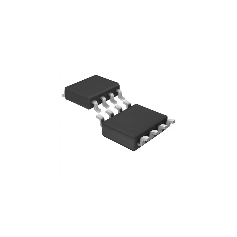
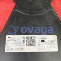
TI OPA657U
Voltage Feedback Amplifier 1 Circuit 8-SOIC


RoHS Status:
Stock Condition: 5459 pcs, New Original
Warranty: 1 Year Ovaga Warranty - Find Out More
0
1
Add To BomOPA657U General Description
The OPA657 device combines a high-gain bandwidth, low-distortion, voltage-feedback operational amplifier with a low-voltage noise JFET-input stage to offer a very high dynamic range amplifier for high-precision ADC (analog-to-digital converter) driving or wideband transimpedance applications. Photodiode applications see improved noise and bandwidth using this decompensated, high-gain bandwidth amplifier.
Very low level signals can be significantly amplified in a single OPA657 gain stage with exceptional bandwidth and accuracy. Having a high 1.6-GHz gain bandwidth product gives greater than 10-MHz signal bandwidths up to gains of 160 V/V (44 dB). The very low input bias current and capacitance supports this performance even for relatively high source impedances.
Broadband photodetector applications benefit from the low-voltage noise JFET inputs for the OPA657. The JFET input contributes virtually no current noise while for broadband applications, a low voltage noise is also required. The low 4.8 nV/√Hz input voltage noise provides exceptional input sensitivity for higher bandwidth applications. The example shown below gives a total equivalent input noise current of 1.8 pA/√Hz over a 10-MHz bandwidth.
Features
- High Gain Bandwidth Product: 1.6 GHz
- High Bandwidth 275 MHz (G = 10)
- Slew Rate 700 V/µs (G = 10, 1-V Step)
- Available in High Grade With Improved DC
Specifications - Operating Temperature Range: –40°C to 85°C
- Low-Input Offset Voltage: ±250 µV
- Low-Input Bias Current: 2 pA
- Low-Input Voltage Noise: 4.8 nV/√Hz
- High-Output Current: 70 mA
- Fast Overdrive Recovery
Specifications
| Parameter | Value | Parameter | Value |
|---|---|---|---|
| Architecture | FET / CMOS Input, Voltage FB | Number of channels | 1 |
| Total supply voltage (+5 V = 5, ±5 V = 10) (min) (V) | 8 | Total supply voltage (+5 V = 5, ±5 V = 10) (max) (V) | 12 |
| GBW (typ) (MHz) | 1600 | BW at Acl (MHz) | 350 |
| Acl, min spec gain (V/V) | 7 | Slew rate (typ) (V/µs) | 700 |
| Vn at flatband (typ) (nV√Hz) | 4.8 | Vn at 1 kHz (typ) (nV√Hz) | 7 |
| Iq per channel (typ) (mA) | 14 | Vos (offset voltage at 25°C) (max) (mV) | 1.8 |
| Rail-to-rail | No | Features | Decompensated |
| Rating | Catalog | Operating temperature range (°C) | -40 to 85 |
| CMRR (typ) (dB) | 89 | Input bias current (max) (pA) | 20 |
| Offset drift (typ) (µV/°C) | 2 | Iout (typ) (mA) | 70 |
| 2nd harmonic (dBc) | 74 | 3rd harmonic (dBc) | 106 |
| Frequency of harmonic distortion measurement (MHz) | 5 |
Shipping
| Shipping Type | Ship Fee | Lead Time | |
|---|---|---|---|
 |
DHL | $20.00-$40.00 (0.50 KG) | 2-5 days |
 |
Fedex | $20.00-$40.00 (0.50 KG) | 2-5 days |
 |
UPS | $20.00-$40.00 (0.50 KG) | 2-5 days |
 |
TNT | $20.00-$40.00 (0.50 KG) | 2-5 days |
 |
EMS | $20.00-$40.00 (0.50 KG) | 2-5 days |
 |
REGISTERED AIR MAIL | $20.00-$40.00 (0.50 KG) | 2-5 days |
Processing Time:Shipping fee depend on different zone and country.
Payment
| Terms of payment | Hand Fee | |
|---|---|---|
 |
Wire Transfer | charge US$30.00 banking fee. |
 |
Paypal | charge 4.0% service fee. |
 |
Credit Card | charge 3.5% service fee. |
 |
Western Union | charge US.00 banking fee. |
 |
Money Gram | charge US$0.00 banking fee. |
Guarantees
1.The electronic components you purchase include 365 Days Warranty, We guarantee product quality.
2.If some of the items you received aren't of perfect quality, we would resiponsibly arrange your refund or replacement. But the items must remain their orginal condition.
Packing
-
![Product Product]()
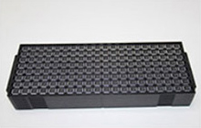
Step1 :Product
-
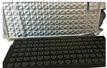
![Vacuum packaging Vacuum packaging]()
Step2 :Vacuum packaging
-
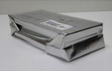
![Anti-static bag Anti-static bag]()
Step3 :Anti-static bag
-
![Individual packaging Individual packaging]()
Step4 :Individual packaging
-
![Packaging boxes Packaging boxes]()
Step5 :Packaging boxes
-
![bar-code shipping tag bar-code shipping tag]()
Step6 :bar-code shipping tag
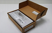
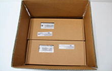
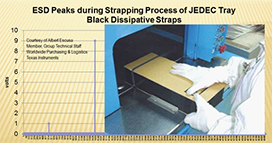
All the products will packing in anti-staticbag. Ship with ESD antistatic protection.
Outside ESD packing’s lable will use ourcompany’s information: Part Mumber, Brand and Quantity.
We will inspect all the goods before shipment,ensure all the products at good condition and ensure the parts are new originalmatch datasheet.
After all the goods are ensure no problems afterpacking, we will packing safely and send by global express. It exhibitsexcellent puncture and tear resistance along with good seal integrity.
We provide high quality products, thoughtful service and after sale guarantee
-
![Product Product]()
We have rich products, can meet your various needs.
-
![quantity quantity]()
Minimum order quantity starts from 1pcs.
-
![shipping shipping]()
Lowest international shipping fee starts from $0.00
-
![guarantee guarantee]()
365 days quality guarantee for all products


