Images are for reference only See Product Specifications
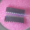
LATTICE LCMXO256C-3TN100C

Flash Programmable Logic Device with 4.9 ns Speed in PQFP100 Package


Brands: Lattice
Mfr.Part #: LCMXO256C-3TN100C
Datasheet: LCMXO256C-3TN100C Datasheet (PDF)
Package/Case: TQFP-100
RoHS Status:
Stock Condition: 7032 pcs, New Original
Product Type: FPGA - Field Programmable Gate Array
Warranty: 1 Year Ovaga Warranty - Find Out More
0
1
*All prices are in USD
| Qty | Unit Price | Ext Price |
|---|---|---|
| 1 | $3.780 | $3.780 |
| 10 | $3.241 | $32.410 |
| 30 | $2.922 | $87.660 |
| 100 | $2.598 | $259.800 |
| 500 | $2.449 | $1224.500 |
| 1000 | $2.382 | $2382.000 |
In Stock:7032 PCS
LCMXO256C-3TN100C General Description
LCMXO256C-3TN100C is a high-performance programmable logic device (PLD) belonging to the Lattice Semiconductor XO2 family. It features 2560 Look-Up Tables (LUTs), 64 Kbits of embedded block RAM, and 72 I/O pins for connectivity. The device operates at a speed grade of -3, meaning it can perform logic operations at a maximum frequency of 3 ns. The LCMXO256C-3TN100C is designed to be used in a variety of applications such as industrial automation, consumer electronics, and communications equipment. It offers low power consumption and high-reliability performance while providing designers with the flexibility to implement complex logic functions. Additionally, the device is housed in a 100-pin TQFP package, making it suitable for small form factor designs. It is also supported by Lattice's design software tools, allowing for easy development and programming of the device.
Features
Application
Specifications
| Parameter | Value | Parameter | Value |
|---|---|---|---|
| Product Category | FPGA - Field Programmable Gate Array | RoHS | Details |
| Series | LCMXO256C | Number of Logic Elements | 256 LE |
| Adaptive Logic Modules - ALMs | 128 ALM | Embedded Memory | 0 bit |
| Number of I/Os | 78 I/O | Supply Voltage - Min | 1.71 V |
| Supply Voltage - Max | 3.465 V | Minimum Operating Temperature | 0 C |
| Maximum Operating Temperature | + 85 C | Mounting Style | SMD/SMT |
| Package / Case | TQFP-100 | Brand | Lattice |
| Distributed RAM | 2 kbit | Height | 1.4 mm |
| Length | 14 mm | Maximum Operating Frequency | 500 MHz |
| Moisture Sensitive | Yes | Number of Logic Array Blocks - LABs | 32 LAB |
| Operating Supply Current | 13 mA | Operating Supply Voltage | 1.8 V/2.5 V/3.3 V |
| Product Type | FPGA - Field Programmable Gate Array | Factory Pack Quantity | 90 |
| Subcategory | Programmable Logic ICs | Total Memory | 2 kbit |
| Width | 14 mm |
Shipping
| Shipping Type | Ship Fee | Lead Time | |
|---|---|---|---|
 |
DHL | $20.00-$40.00 (0.50 KG) | 2-5 days |
 |
Fedex | $20.00-$40.00 (0.50 KG) | 2-5 days |
 |
UPS | $20.00-$40.00 (0.50 KG) | 2-5 days |
 |
TNT | $20.00-$40.00 (0.50 KG) | 2-5 days |
 |
EMS | $20.00-$40.00 (0.50 KG) | 2-5 days |
 |
REGISTERED AIR MAIL | $20.00-$40.00 (0.50 KG) | 2-5 days |
Processing Time:Shipping fee depend on different zone and country.
Payment
| Terms of payment | Hand Fee | |
|---|---|---|
 |
Wire Transfer | charge US$30.00 banking fee. |
 |
Paypal | charge 4.0% service fee. |
 |
Credit Card | charge 3.5% service fee. |
 |
Western Union | charge US.00 banking fee. |
 |
Money Gram | charge US$0.00 banking fee. |
Guarantees
1.The electronic components you purchase include 365 Days Warranty, We guarantee product quality.
2.If some of the items you received aren't of perfect quality, we would resiponsibly arrange your refund or replacement. But the items must remain their orginal condition.
Packing
-

Step1 :Product
-

Step2 :Vacuum packaging
-

Step3 :Anti-static bag
-

Step4 :Individual packaging
-

Step5 :Packaging boxes
-

Step6 :bar-code shipping tag


All the products will packing in anti-staticbag. Ship with ESD antistatic protection.
Outside ESD packing’s lable will use ourcompany’s information: Part Mumber, Brand and Quantity.
We will inspect all the goods before shipment,ensure all the products at good condition and ensure the parts are new originalmatch datasheet.
After all the goods are ensure no problems afterpacking, we will packing safely and send by global express. It exhibitsexcellent puncture and tear resistance along with good seal integrity.


Part points
-
LCMXO256C-3TN100C is a low-cost, low-power, high-performance FPGA chip from Lattice Semiconductor. It features 2560 Look-Up Tables (LUTs), 17,600 bits of Embedded Block RAM, and 94 user I/O pins. It is ideal for applications requiring high-speed processing with minimal power consumption.
-
Equivalent
The equivalent products of LCMXO256C-3TN100C are the Lattice ICE40 and ICE5LP-FPGA families, as well as the Xilinx Spartan-6 series and the Altera Cyclone III series of FPGA chips. These chips offer similar capabilities and performance to the LCMXO256C-3TN100C. -
Features
LCMXO256C-3TN100C is a low-cost, low-power FPGA with 2560 Look-Up Tables (LUTs) and 4000 system gates. It features 108 Kbits of embedded block RAM, various I/O options, and 36 user-configurable I/O pins. The device operates at a 3.3V voltage and has numerous security features to protect intellectual property. -
Pinout
LCMXO256C-3TN100C is a Lattice MachXO256C FPGA with 100-pin TQFP package. It has 100 pins for connecting to external components and purposes such as input/output, clock signals, power, and configuration. -
Manufacturer
LCMXO256C-3TN100C is manufactured by Lattice Semiconductor Corporation, an American company that designs and manufactures programmable logic devices. Lattice Semiconductor provides programmable logic devices, development software, and IP core design services to customers in the consumer, communications, industrial, computing, and automotive markets. -
Application Field
LCMXO256C-3TN100C is commonly used in applications such as low-power industrial automation, telecommunications, consumer electronics, and automotive systems. It is suitable for applications requiring high levels of integration, low power consumption, and small form factor design. -
Package
The LCMXO256C-3TN100C chip is a Field Programmable Gate Array (FPGA) with a 100-pin TQFP (Thin Quad Flat Package) form factor and a size of 14mm x 14mm.


We provide high quality products, thoughtful service and after sale guarantee
-

We have rich products, can meet your various needs.
-

Minimum order quantity starts from 1pcs.
-

Lowest international shipping fee starts from $0.00
-

365 days quality guarantee for all products