Images are for reference only See Product Specifications
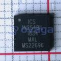
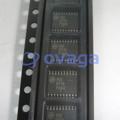
CY7B991V-5JXI

PLL Based Clock Driver, 7B Series, 4 True Output(s), 0 Inverted Output(s), PQCC32


Brands: CYPRESS
Mfr.Part #: CY7B991V-5JXI
Datasheet: CY7B991V-5JXI Datasheet (PDF)
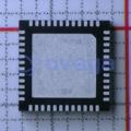
Package/Case: PLCC32
RoHS Status:
Stock Condition: 401 pcs, New Original
Product Type: Phase Locked Loops
Warranty: 1 Year Ovaga Warranty - Find Out More
0
1
*All prices are in USD
| Qty | Unit Price | Ext Price |
|---|---|---|
| 1 | $2.601 | $2.601 |
| 200 | $1.007 | $201.400 |
| 500 | $0.971 | $485.500 |
| 1000 | $0.955 | $955.000 |
In Stock:401 PCS
CY7B991V-5JXI General Description
IC, CLOCK BUFFER, 80MHz, LCC-32; Clock I; IC, CLOCK BUFFER, 80MHz, LCC-32; Clock IC Type:Clock Buffer; Frequency:80MHz; No. of Outputs:8; Supply Current:100mA; Supply Voltage Range:2.97V to 3.63V; Digital IC Case Style:LCC; No. of Pins:32
Specifications
| Parameter | Value | Parameter | Value |
|---|---|---|---|
| Product Category | Phase Locked Loops - PLL | RoHS | Details |
| Type | Zero Delay Programmable PLL Clock Buffer | Number of Circuits | 1 Circuit |
| Output Frequency Range | 3.75 MHz to 80 MHz | Supply Voltage - Max | 3.63 V |
| Supply Voltage - Min | 2.97 V | Technology | Si |
| Minimum Operating Temperature | - 40 C | Maximum Operating Temperature | + 85 C |
| Mounting Style | SMD/SMT | Package / Case | PLCC-32 |
| Brand | Infineon Technologies | Height | 2.67 mm |
| Length | 14.05 mm | Moisture Sensitive | Yes |
| Operating Supply Voltage | 3.3 V | Product Type | PLLs - Phase Locked Loops |
| Series | CY7B991V | Factory Pack Quantity | 300 |
| Subcategory | Wireless & RF Integrated Circuits | Tradename | RoboClock |
| Width | 11.5 mm |
Shipping
| Shipping Type | Ship Fee | Lead Time | |
|---|---|---|---|
 |
DHL | $20.00-$40.00 (0.50 KG) | 2-5 days |
 |
Fedex | $20.00-$40.00 (0.50 KG) | 2-5 days |
 |
UPS | $20.00-$40.00 (0.50 KG) | 2-5 days |
 |
TNT | $20.00-$40.00 (0.50 KG) | 2-5 days |
 |
EMS | $20.00-$40.00 (0.50 KG) | 2-5 days |
 |
REGISTERED AIR MAIL | $20.00-$40.00 (0.50 KG) | 2-5 days |
Processing Time:Shipping fee depend on different zone and country.
Payment
| Terms of payment | Hand Fee | |
|---|---|---|
 |
Wire Transfer | charge US$30.00 banking fee. |
 |
Paypal | charge 4.0% service fee. |
 |
Credit Card | charge 3.5% service fee. |
 |
Western Union | charge US.00 banking fee. |
 |
Money Gram | charge US$0.00 banking fee. |
Guarantees
1.The electronic components you purchase include 365 Days Warranty, We guarantee product quality.
2.If some of the items you received aren't of perfect quality, we would resiponsibly arrange your refund or replacement. But the items must remain their orginal condition.
Packing
-

Step1 :Product
-

Step2 :Vacuum packaging
-

Step3 :Anti-static bag
-

Step4 :Individual packaging
-

Step5 :Packaging boxes
-

Step6 :bar-code shipping tag


All the products will packing in anti-staticbag. Ship with ESD antistatic protection.
Outside ESD packing’s lable will use ourcompany’s information: Part Mumber, Brand and Quantity.
We will inspect all the goods before shipment,ensure all the products at good condition and ensure the parts are new originalmatch datasheet.
After all the goods are ensure no problems afterpacking, we will packing safely and send by global express. It exhibitsexcellent puncture and tear resistance along with good seal integrity.


Part points
-
The CY7B991V-5JXI chip is a high-performance synchronous FIFO (First-In, First-Out) memory device manufactured by Cypress Semiconductor. It features a 256 x 9-bit memory array with an internal counter for addressing. The chip operates at a maximum frequency of 100 MHz and is commonly used in applications requiring data buffering and synchronization.
-
Equivalent
The CY7B991V-5JXI chip is an obsolete part, and finding exact equivalents may be difficult. However, similar functionality may be found in modern interface ICs like those from Texas Instruments, Maxim Integrated, or Analog Devices. Consult datasheets and technical specifications for compatibility. -
Features
The CY7B991V-5JXI is a high-speed, low-skew CMOS clock buffer with 10 outputs. It features a 1:10 fanout and operates at up to 133 MHz. It offers low output skew and jitter, making it suitable for demanding clock distribution applications in various systems. -
Pinout
The CY7B991V-5JXI is a 28-pin CMOS synchronous FIFO memory chip. It serves as a buffer for data transfer between asynchronous systems, with a maximum data rate of 50 MHz. Key functions include data input/output, control signals, and clock synchronization. -
Manufacturer
The CY7B991V-5JXI is manufactured by Cypress Semiconductor Corporation, which is a semiconductor design and manufacturing company. They specialize in providing a wide range of high-performance integrated circuits for various industries, including automotive, industrial, consumer electronics, and communications. Cypress Semiconductor Corporation is headquartered in San Jose, California, and is known for its innovative solutions and advanced technologies. -
Application Field
The CY7B991V-5JXI is a programmable clock generator typically used in networking, telecommunications, and industrial applications. It provides flexibility in generating various clock signals, making it suitable for applications requiring precise timing control, such as routers, switches, base stations, and test equipment. -
Package
The CY7B991V-5JXI chip typically comes in a 28-pin PLCC (Plastic Leaded Chip Carrier) package with a surface-mount form factor.


We provide high quality products, thoughtful service and after sale guarantee
-

We have rich products, can meet your various needs.
-

Minimum order quantity starts from 1pcs.
-

Lowest international shipping fee starts from $0.00
-

365 days quality guarantee for all products