Images are for reference only See Product Specifications
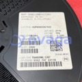
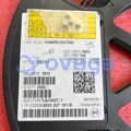
CD4011BM
The CD4011BM is a versatile integrated circuit that features four independent 2-input NAND gates, making it ideal for logic circuit design


Brands: Texas Instruments
Mfr.Part #: CD4011BM
Datasheet: CD4011BM Datasheet (PDF)
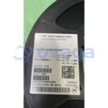
Package/Case: SOIC (D)-14
RoHS Status:
Stock Condition: 7399 pcs, New Original
Warranty: 1 Year Ovaga Warranty - Find Out More
0
1
Add To BomCD4011BM General Description
CD4011B, CD4012B, and CD4023B NAND gates provide the system designer with direct implementation of the NAND function and supplement the existing family of CMOS gates. All inputs and outputs are buffered.
The CD4011B, CD4012B, and CD4023B types are supplied in 14-lead hermetic dual-in-line ceramic packages (F3A suffix), 14-lead dual-in-line plastic packages (E suffix), 14-lead small-outline packages (M, MT, M96, and NSR suffixes), and 14-lead thin shrink small-outline packages (PWR suffix). The CD4011B and CD4023B types also are supplied in 14-lead thin shrink small-outline packages (PW suffix).
Features
- Propagation delay time = 60 ns (typ.) at CL = 50 pF, VDD = 10 V
- Buffered inputs and outputs
- Standardized symmetrical output characteristics
- Maximum input current of 1 µA at 18 V over-full package temperature range; 100 nA at 18 V and 25°C
- 100% tested for quiescent current at 20 V
- 5-V, 10-V, and 15-V parametric ratings
- Noise margin (over full package temperature range:
1 V at VDD = 5 V
2 V at VDD = 10 V
2.5 at VDD = 15 V - Meets all requirements of JEDEC Tentative Standard No. 13B, "Standard Specifications for Description of "B" Series CMOS Devices"
Quad 2 Input—CD4011B
Dual 4 Input—CD4012B
Triple 3 Input—CD4023B
Data sheet acquired from Harris Semiconductor.
Application
Specifications
| Parameter | Value | Parameter | Value |
|---|---|---|---|
| Technology family | CD4000 | Supply voltage (min) (V) | 3 |
| Supply voltage (max) (V) | 18 | Number of channels | 4 |
| Inputs per channel | 2 | IOL (max) (mA) | 6.8 |
| IOH (max) (mA) | -6.8 | Input type | Standard CMOS |
| Output type | Push-Pull | Features | Standard speed (tpd > 50ns) |
| Data rate (max) (MBps) | 8 | Rating | Catalog |
| Operating temperature range (°C) | -55 to 125 |
Shipping
| Shipping Type | Ship Fee | Lead Time | |
|---|---|---|---|
 |
DHL | $20.00-$40.00 (0.50 KG) | 2-5 days |
 |
Fedex | $20.00-$40.00 (0.50 KG) | 2-5 days |
 |
UPS | $20.00-$40.00 (0.50 KG) | 2-5 days |
 |
TNT | $20.00-$40.00 (0.50 KG) | 2-5 days |
 |
EMS | $20.00-$40.00 (0.50 KG) | 2-5 days |
 |
REGISTERED AIR MAIL | $20.00-$40.00 (0.50 KG) | 2-5 days |
Processing Time:Shipping fee depend on different zone and country.
Payment
| Terms of payment | Hand Fee | |
|---|---|---|
 |
Wire Transfer | charge US$30.00 banking fee. |
 |
Paypal | charge 4.0% service fee. |
 |
Credit Card | charge 3.5% service fee. |
 |
Western Union | charge US.00 banking fee. |
 |
Money Gram | charge US$0.00 banking fee. |
Guarantees
1.The electronic components you purchase include 365 Days Warranty, We guarantee product quality.
2.If some of the items you received aren't of perfect quality, we would resiponsibly arrange your refund or replacement. But the items must remain their orginal condition.
Packing
-

Step1 :Product
-

Step2 :Vacuum packaging
-

Step3 :Anti-static bag
-

Step4 :Individual packaging
-

Step5 :Packaging boxes
-

Step6 :bar-code shipping tag


All the products will packing in anti-staticbag. Ship with ESD antistatic protection.
Outside ESD packing’s lable will use ourcompany’s information: Part Mumber, Brand and Quantity.
We will inspect all the goods before shipment,ensure all the products at good condition and ensure the parts are new originalmatch datasheet.
After all the goods are ensure no problems afterpacking, we will packing safely and send by global express. It exhibitsexcellent puncture and tear resistance along with good seal integrity.


We provide high quality products, thoughtful service and after sale guarantee
-

We have rich products, can meet your various needs.
-

Minimum order quantity starts from 1pcs.
-

Lowest international shipping fee starts from $0.00
-

365 days quality guarantee for all products