Images are for reference only See Product Specifications
TI TPS61291DRVR

Switching Voltage Regulators Low Iq Boost Cnvrtr


Brands: TI
Mfr.Part #: TPS61291DRVR
Datasheet: TPS61291DRVR Datasheet (PDF)
Package/Case: WSON6
RoHS Status:
Stock Condition: 9000 pcs, New Original
Product Type: Voltage Regulators - DC DC Switching Regulators
Warranty: 1 Year Ovaga Warranty - Find Out More
0
1
*All prices are in USD
| Qty | Unit Price | Ext Price |
|---|---|---|
| 1 | $0.448 | $0.448 |
| 10 | $0.361 | $3.610 |
| 30 | $0.322 | $9.660 |
| 100 | $0.274 | $27.400 |
| 500 | $0.243 | $121.500 |
| 1000 | $0.229 | $229.000 |
In Stock:9000 PCS
TPS61291DRVR General Description
The TPS61291 is a boost converter with pin selectable output voltages and an integrated bypass mode. In bypass operation, the device provides a direct path from the input to the system and allows a low power micro controller (MCU) such as the MSP430 to operate directly from a single 3V Li-MnO2 battery or dual alkaline battery cells.
In bypass mode the integrated feedback divider network for boost mode operation is disconnected from the output and the quiescent current consumption drops down to only 15nA (typical).
In boost mode the device provides a minimum output current of 200mA at 3.3V VOUT from 1.8V VIN. The boost mode is used for system components which require a regulated supply voltage and cannot directly operate from the input source. The boost converter is based on a current-mode controller using synchronous rectification to obtain maximum efficiency and consumes typically 5.7µA from the output. During startup of the boost converter, the VSEL pin is read out and the integrated feedback network sets the output voltage to 2.5V, 3V or 3.3V.
Bypass mode or boost mode operation is controlled by the system via the EN/BYP pin.
The device integrates an enhanced bypass mode control to prevent charge, stored in the output capacitor during boost mode operation, from flowing back to the input and charging the battery.
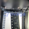
The device is packaged in a small 6-pin SON package (DRV) measuring 2.0mm × 2.0mm × 0.75mm.
Features
- Input Voltage Range 0.9V to 5V
- Startup Voltage 1.5V at 20mA Load
- Pin Selectable Output Voltages:
3.3V, 3V, 2.5V - 15nA typical Quiescent Current in
Bypass Mode - 5.7µA typical Quiescent Current in
Boost Mode - Bypass Switch from VIN to VOUT
- IOUT > 200mA at 3.3V VOUT,
VIN = 1.8V - Internal Feedback Divider Disconnect
(Bypass Mode) - Controlled Bypass Transition Prevents
Reverse Current into Battery - Power-Save Mode at Light Loads
- Overtemperature Protection
- Redundant Overvoltage Protection
- Small 2mm × 2mm SON 6-pin package
Specifications
| Parameter | Value | Parameter | Value |
|---|---|---|---|
| Topology | Boost | Vin (min) (V) | 0.9 |
| Vin (max) (V) | 5 | Vout (min) (V) | 2.5 |
| Vout (max) (V) | 3.3 | Switch current limit (typ) (A) | 1 |
| Type | Converter | Regulated outputs (#) | 1 |
| Switching frequency (min) (kHz) | 2300 | Switching frequency (max) (kHz) | 2300 |
| Iq (typ) (mA) | 0.005 | Features | Bypass Mode Pass-through Mode, Synchronous Rectification |
| Duty cycle (max) (%) | 90 | Operating temperature range (°C) | -40 to 85 |
| Rating | Catalog |
Shipping
| Shipping Type | Ship Fee | Lead Time | |
|---|---|---|---|
 |
DHL | $20.00-$40.00 (0.50 KG) | 2-5 days |
 |
Fedex | $20.00-$40.00 (0.50 KG) | 2-5 days |
 |
UPS | $20.00-$40.00 (0.50 KG) | 2-5 days |
 |
TNT | $20.00-$40.00 (0.50 KG) | 2-5 days |
 |
EMS | $20.00-$40.00 (0.50 KG) | 2-5 days |
 |
REGISTERED AIR MAIL | $20.00-$40.00 (0.50 KG) | 2-5 days |
Processing Time:Shipping fee depend on different zone and country.
Payment
| Terms of payment | Hand Fee | |
|---|---|---|
 |
Wire Transfer | charge US$30.00 banking fee. |
 |
Paypal | charge 4.0% service fee. |
 |
Credit Card | charge 3.5% service fee. |
 |
Western Union | charge US.00 banking fee. |
 |
Money Gram | charge US$0.00 banking fee. |
Guarantees
1.The electronic components you purchase include 365 Days Warranty, We guarantee product quality.
2.If some of the items you received aren't of perfect quality, we would resiponsibly arrange your refund or replacement. But the items must remain their orginal condition.
Packing
-

Step1 :Product
-

Step2 :Vacuum packaging
-

Step3 :Anti-static bag
-

Step4 :Individual packaging
-

Step5 :Packaging boxes
-

Step6 :bar-code shipping tag


All the products will packing in anti-staticbag. Ship with ESD antistatic protection.
Outside ESD packing’s lable will use ourcompany’s information: Part Mumber, Brand and Quantity.
We will inspect all the goods before shipment,ensure all the products at good condition and ensure the parts are new originalmatch datasheet.
After all the goods are ensure no problems afterpacking, we will packing safely and send by global express. It exhibitsexcellent puncture and tear resistance along with good seal integrity.


Part points
-
The TPS61291DRVR is a power management integrated circuit (IC) designed for efficient voltage boosting in battery-powered applications. It can convert a low input voltage into a higher output voltage, making it useful for boosting battery voltage for devices such as smartphones, tablets, and wearable devices. It features high efficiency, low quiescent current, and various protection features to ensure reliable and efficient power conversion.
-
Equivalent
Some equivalent products to the TPS61291DRVR chip include TPS61292DRVT, TPS610995DRVR, and TPS61292RTJT. These chips are also voltage boost converters with similar features and functionality. It is recommended to consult the datasheets of these chips for further details and compatibility. -
Features
The TPS61291DRVR is a boost converter with a wide input voltage range, capable of boosting voltages up to 12V. It has a high efficiency, low quiescent current, and supports load disconnect during shutdown. Additionally, it has integrated overvoltage protection, power save mode, and a small package size, making it suitable for portable and battery-powered applications. -
Pinout
The TPS61291DRVR is a 10-pin buck-boost converter IC. It has the following pin functions: EN (Enable), VIN (Input Voltage), GND (Ground), NC (No Connect), PG (Power Good), FB (Feedback), LIM (Limit), VSEL (Voltage Select), VOUT (Output Voltage), and NC (No Connect). -
Manufacturer
The manufacturer of the TPS61291DRVR is Texas Instruments. It is a multinational semiconductor and technology company involved in designing and manufacturing various electronic components and systems for a wide range of applications in industries such as automotive, industrial, and consumer electronics. -
Application Field
The TPS61291DRVR is a constant current boost converter used for compact power management solutions. It is commonly used in portable devices such as smartphones, tablets, and wearable devices to efficiently boost low battery voltages to higher voltages required by the system components. The TPS61291DRVR is also utilized in applications where space is limited and a low power boost converter is needed. -
Package
The TPS61291DRVR chip is available in a DSBGA-6 package, has a round form, and its size is approximately 1.5 mm x 1.5 mm.


We provide high quality products, thoughtful service and after sale guarantee
-

We have rich products, can meet your various needs.
-

Minimum order quantity starts from 1pcs.
-

Lowest international shipping fee starts from $0.00
-

365 days quality guarantee for all products