Images are for reference only See Product Specifications
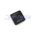
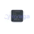
TMS32C6415EZLZ6E3

C64x fixed point DSP- up to 720MHz, McBSP, PCI


Brands: TEXAS INSTRUMENTS INC
Mfr.Part #: TMS32C6415EZLZ6E3
Datasheet: TMS32C6415EZLZ6E3 Datasheet (PDF)
Package/Case: FCBGA-532
RoHS Status:
Stock Condition: 6554 pcs, New Original
Product Type: Digital Signal Processors & Controllers - DSP, DSC
Warranty: 1 Year Ovaga Warranty - Find Out More
0
1
*All prices are in USD
| Qty | Unit Price | Ext Price |
|---|---|---|
| 1 | $182.327 | $182.327 |
| 200 | $70.559 | $14111.800 |
| 500 | $68.078 | $34039.000 |
| 1000 | $66.853 | $66853.000 |
In Stock:6554 PCS
TMS32C6415EZLZ6E3 General Description
The TMS320C64x DSPs (including the TMS320C6414, TMS320C6415, and TMS320C6416 devices) are the highest-performance fixed-point DSP generation in the TMS320C6000 DSP platform. The TMS320C64x (C64x) device is based on the second-generation high-performance, advanced VelociTI very-long-instruction-word (VLIW) architecture (VelociTI.2 developed by Texas Instruments (TI), making these DSPs an excellent choice for multichannel and multifunction applications. The C64x is a code-compatible member of the C6000 DSP platform.
With performance of up to 5760 million instructions per second (MIPS) at a clock rate of 720 MHz, the C64x devices offer cost-effective solutions to high-performance DSP programming challenges. The C64x DSPs possess the operational flexibility of high-speed controllers and the numerical capability of array processors. The C64x DSP core processor has 64 general-purpose registers of 32-bit word length and eight highly independent functional unitstwo multipliers for a 32-bit result and six arithmetic logic units (ALUs) with VelociTI.2 extensions. The VelociTI.2 extensions in the eight functional units include new instructions to accelerate the performance in key applications and extend the parallelism of the VelociTI architecture. The C64x can produce four 16-bit multiply-accumulates (MACs) per cycle for a total of 2880 million MACs per second (MMACS), or eight 8-bit MACs per cycle for a total of 5760 MMACS. The C64x DSP also has application-specific hardware logic, on-chip memory, and additional on-chip peripherals similar to the other C6000 DSP platform devices.
The C6416 device has two high-performance embedded coprocessors [Viterbi Decoder Coprocessor (VCP) and Turbo Decoder Coprocessor (TCP)] that significantly speed up channel-decoding operations on-chip. The VCP operating at CPU clock divided-by-4 can decode over 600 7.95-Kbps adaptive multi-rate (AMR) [K = 9, R = 1/3] voice channels. The VCP supports constraint lengths K = 5, 6, 7, 8, and 9, rates R = 1/2, 1/3, and 1/4, and flexible polynomials, while generating hard decisions or soft decisions. The TCP operating at CPU clock divided-by-2 can decode up to forty-three 384-Kbps or seven 2-Mbps turbo encoded channels (assuming 6 iterations). The TCP implements the max*log-map algorithm and is designed to support all polynomials and rates required by Third-Generation Partnership Projects (3GPP and 3GPP2), with fully programmable frame length and turbo interleaver. Decoding parameters such as the number of iterations and stopping criteria are also programmable. Communications between the VCP/TCP and the CPU are carried out through the EDMA controller.
The C64x uses a two-level cache-based architecture and has a powerful and diverse set of peripherals. The Level 1 program cache (L1P) is a 128-Kbit direct mapped cache and the Level 1 data cache (L1D) is a 128-Kbit 2-way set-associative cache. The Level 2 memory/cache (L2) consists of an 8-Mbit memory space that is shared between program and data space. L2 memory can be configured as mapped memory or combinations of cache (up to 256K bytes) and mapped memory. The peripheral set includes three multichannel buffered serial ports (McBSPs); an 8-bit Universal Test and Operations PHY Interface for Asynchronous Transfer Mode (ATM) Slave [UTOPIA Slave] port (C6415/C6416 only); three 32-bit general-purpose timers; a user-configurable 16-bit or 32-bit host-port interface (HPI16/HPI32); a peripheral component interconnect (PCI) [C6415/C6416 only]; a general-purpose input/output port (GPIO) with 16 GPIO pins; and two glueless external memory interfaces (64-bit EMIFA and 16-bit EMIFB), both of which are capable of interfacing to synchronous and asynchronous memories and peripherals.
The C64x has a complete set of development tools which includes: an advanced C compiler with C64x-specific enhancements, an assembly optimizer to simplify programming and scheduling, and a Windows debugger interface for visibility into source code execution.
Features
- Highest-Performance Fixed-Point Digital Signal Processors (DSPs)
- 2-, 1.67-, 1.39-ns Instruction Cycle Time
- 500-, 600-, 720-MHz Clock Rate
- Eight 32-Bit Instructions/Cycle
- Twenty-Eight Operations/Cycle
- 4000, 4800, 5760 MIPS
- Fully Software-Compatible With C62x™
- C6414/15/16 Devices Pin-Compatible
- VelociTI.2™ Extensions to VelociTI™ Advanced Very-Long-Instruction-Word (VLIW) TMS320C64x™ DSP Core
- Eight Highly Independent Functional Units With VelociTI.2™ Extensions:
- Six ALUs (32-/40-Bit), Each Supports Single 32-Bit, Dual 16-Bit, or Quad 8-Bit Arithmetic per Clock Cycle
- Two Multipliers Support Four 16 x 16-Bit Multiplies (32-Bit Results) per Clock Cycle or Eight 8 x 8-Bit Multiplies (16-Bit Results) per Clock Cycle
- Non-Aligned Load-Store Architecture
- 64 32-Bit General-Purpose Registers
- Instruction Packing Reduces Code Size
- All Instructions Conditional
- Eight Highly Independent Functional Units With VelociTI.2™ Extensions:
- Instruction Set Features
- Byte-Addressable (8-/16-/32-/64-Bit Data)
- 8-Bit Overflow Protection
- Bit-Field Extract, Set, Clear
- Normalization, Saturation, Bit-Counting
- VelociTI.2™ Increased Orthogonality
- Viterbi Decoder Coprocessor (VCP) [C6416]
- Supports Over 600 7.95-Kbps AMR
- Programmable Code Parameters
- Turbo Decoder Coprocessor (TCP) [C6416]
- Supports up to 7 2-Mbps or 43 384-Kbps 3GPP (6 Iterations)
- Programmable Turbo Code and Decoding Parameters
- L1/L2 Memory Architecture
- 128K-Bit (16K-Byte) L1P Program Cache (Direct Mapped)
- 128K-Bit (16K-Byte) L1D Data Cache (2-Way Set-Associative)
- 8M-Bit (1024K-Byte) L2 Unified Mapped RAM/Cache (Flexible Allocation)
- Two External Memory Interfaces (EMIFs)
- One 64-Bit (EMIFA), One 16-Bit (EMIFB)
- Glueless Interface to Asynchronous Memories (SRAM and EPROM) and Synchronous Memories (SDRAM, SBSRAM, ZBT SRAM, and FIFO)
- 1280M-Byte Total Addressable External Memory Space
- Enhanced Direct-Memory-Access (EDMA) Controller (64 Independent Channels)
- Host-Port Interface (HPI)
- User-Configurable Bus Width (32-/16-Bit)
- 32-Bit/33-MHz, 3.3-V PCI Master/Slave Interface Conforms to PCI Specification 2.2 [C6415/C6416 ]
- Three PCI Bus Address Registers:
Prefetchable Memory
Non-Prefetchable Memory I/O - Four-Wire Serial EEPROM Interface
- PCI Interrupt Request Under DSP Program Control
- DSP Interrupt Via PCI I/O Cycle
- Three PCI Bus Address Registers:
- Three Multichannel Buffered Serial Ports
- Direct Interface to T1/E1, MVIP, SCSA Framers
- Up to 256 Channels Each
- ST-Bus-Switching-, AC97-Compatible
- Serial Peripheral Interface (SPI) Compatible (Motorola™)
- Three 32-Bit General-Purpose Timers
- Universal Test and Operations PHY Interface for ATM (UTOPIA) [C6415/C6416]
- UTOPIA Level 2 Slave ATM Controller
- 8-Bit Transmit and Receive Operations up to 50 MHz per Direction
- User-Defined Cell Format up to 64 Bytes
- Sixteen General-Purpose I/O (GPIO) Pins
- Flexible PLL Clock Generator
- IEEE-1149.1 (JTAG) Boundary-Scan-Compatible
- 532-Pin Ball Grid Array (BGA) Package (GLZ, ZLZ and CLZ Suffixes), 0.8-mm Ball Pitch
- 0.13-µm/6-Level Cu Metal Process (CMOS)
- 3.3-V I/Os, 1.2-V/1.25-V Internal (500 MHz)
- 3.3-V I/Os, 1.4-V Internal (600 and 720 MHz)
C62x, VelociTI.2, VelociTI, and TMS320C64x are trademarks of Texas Instruments.
Motorola is a trademark of Motorola, Inc.
IEEE Standard 1149.1-1990 Standard-Test-Access Port and Boundary Scan Architecture.
TMS320C6000, C64x, and C6000 are trademarks of Texas Instruments.
Windows is a registered trademark of the Microsoft Corporation.
Other trademarks are the property of their respective owners.
Throughout the remainder of this document, the TMS320C6414, TMS320C6415, and TMS320C6416 shall be referred to as TMS320C64x or C64x where generic, and where specific, their individual full device part numbers will be used or abbreviated as C6414, C6415, or C6416.
These C64xdevices have two EMIFs (64-bit EMIFA and 16-bit EMIFB). The prefix "A" in front of a signal name indicates it is an EMIFA signal whereas a prefix "B" in front of a signal name indicates it is an EMIFB signal. Throughout the rest of this document, in generic EMIF areas of discussion, the prefix "A" or "B" may be omitted from the signal name.
Specifications
| Parameter | Value | Parameter | Value |
|---|---|---|---|
| Source Content uid | TMS32C6415EZLZ6E3 | Pbfree Code | Yes |
| Rohs Code | No | Part Life Cycle Code | Active |
| Ihs Manufacturer | TEXAS INSTRUMENTS INC | Part Package Code | BGA |
| Package Description | HFBGA, BGA532,26X26,32 | Pin Count | 532 |
| Reach Compliance Code | compliant | ECCN Code | 3A991.A.2 |
| HTS Code | 8542.31.00.01 | Samacsys Manufacturer | Texas Instruments |
| Additional Feature | ALSO REQUIRES 3.3VI/O SUPPLY | Address Bus Width | 32 |
| Barrel Shifter | NO | Bit Size | 32 |
| Boundary Scan | YES | Clock Frequency-Max | 75.18 MHz |
| External Data Bus Width | 64 | Format | FIXED POINT |
| Integrated Cache | YES | Internal Bus Architecture | MULTIPLE |
| JESD-30 Code | S-PBGA-B532 | JESD-609 Code | e1 |
| Length | 23 mm | Low Power Mode | YES |
| Moisture Sensitivity Level | 4 | Number of DMA Channels | 64 |
| Number of External Interrupts | 4 | Number of Terminals | 532 |
| Number of Timers | 3 | Operating Temperature-Max | 90 °C |
| Operating Temperature-Min | Package Body Material | PLASTIC/EPOXY | |
| Package Code | HFBGA | Package Equivalence Code | BGA532,26X26,32 |
| Package Shape | SQUARE | Package Style | GRID ARRAY, HEAT SINK/SLUG, FINE PITCH |
| Peak Reflow Temperature (Cel) | 260 | Power Supplies | 1.4,3.3 V |
| Qualification Status | Not Qualified | RAM (words) | 16384 |
| Seated Height-Max | 3.3 mm | Supply Current-Max | 125 mA |
| Supply Voltage-Max | 1.44 V | Supply Voltage-Min | 1.36 V |
| Supply Voltage-Nom | 1.4 V | Surface Mount | YES |
| Technology | CMOS | Temperature Grade | OTHER |
| Terminal Finish | Tin/Silver/Copper (Sn/Ag/Cu) | Terminal Form | BALL |
| Terminal Pitch | 0.8 mm | Terminal Position | BOTTOM |
| Time@Peak Reflow Temperature-Max (s) | NOT SPECIFIED | Width | 23 mm |
| uPs/uCs/Peripheral ICs Type | DIGITAL SIGNAL PROCESSOR, OTHER |
Shipping
| Shipping Type | Ship Fee | Lead Time | |
|---|---|---|---|
 |
DHL | $20.00-$40.00 (0.50 KG) | 2-5 days |
 |
Fedex | $20.00-$40.00 (0.50 KG) | 2-5 days |
 |
UPS | $20.00-$40.00 (0.50 KG) | 2-5 days |
 |
TNT | $20.00-$40.00 (0.50 KG) | 2-5 days |
 |
EMS | $20.00-$40.00 (0.50 KG) | 2-5 days |
 |
REGISTERED AIR MAIL | $20.00-$40.00 (0.50 KG) | 2-5 days |
Processing Time:Shipping fee depend on different zone and country.
Payment
| Terms of payment | Hand Fee | |
|---|---|---|
 |
Wire Transfer | charge US$30.00 banking fee. |
 |
Paypal | charge 4.0% service fee. |
 |
Credit Card | charge 3.5% service fee. |
 |
Western Union | charge US.00 banking fee. |
 |
Money Gram | charge US$0.00 banking fee. |
Guarantees
1.The electronic components you purchase include 365 Days Warranty, We guarantee product quality.
2.If some of the items you received aren't of perfect quality, we would resiponsibly arrange your refund or replacement. But the items must remain their orginal condition.
Packing
-

Step1 :Product
-

Step2 :Vacuum packaging
-

Step3 :Anti-static bag
-

Step4 :Individual packaging
-

Step5 :Packaging boxes
-

Step6 :bar-code shipping tag


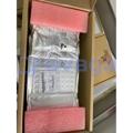
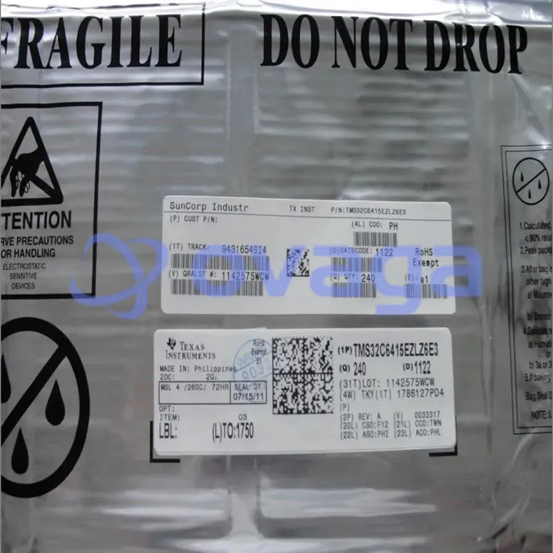
All the products will packing in anti-staticbag. Ship with ESD antistatic protection.
Outside ESD packing’s lable will use ourcompany’s information: Part Mumber, Brand and Quantity.
We will inspect all the goods before shipment,ensure all the products at good condition and ensure the parts are new originalmatch datasheet.
After all the goods are ensure no problems afterpacking, we will packing safely and send by global express. It exhibitsexcellent puncture and tear resistance along with good seal integrity.


Part points
-
The TMS32C6415EZLZ6E3 chip is a digital signal processor (DSP) from Texas Instruments, designed for high-performance audio and voice applications. It features a 32-bit RISC core running at up to 600 MHz, dual multiply-accumulate units, and a variety of on-chip peripherals. The chip is ideal for applications requiring real-time processing and low power consumption.
-
Equivalent
Some equivalent products of the TMS32C6415EZLZ6E3 chip are the TMS320C6414T, TMS320C6416T, and TMS320C6416EZLZ6E3. These chips are all from the same TMS320C64x series by Texas Instruments and are suitable for use in various digital signal processing applications. -
Features
The TMS320C6415EZLZ6E3 is a digital signal processor (DSP) from Texas Instruments. It features a fixed-point architecture, operates at 720 MHz, has 6KB of L1 instruction cache and 6KB of L1 data cache, supports multiple data types, and includes various peripherals for connectivity and processing. -
Pinout
The TMS32C6415EZLZ6E3 is a digital signal processor (DSP) by Texas Instruments. It has 532 pins. Functions include processing audio, video, and other real-time data with high performance and low power consumption. -
Manufacturer
The TMS32C6415EZLZ6E3 is manufactured by Texas Instruments (TI). TI is a leading semiconductor company, specializing in designing and manufacturing a wide range of integrated circuits and related products for various applications, including consumer electronics, automotive, industrial, and communications. -
Application Field
The TMS320C6415EZLZ6E3 is commonly used in digital signal processing applications such as audio processing, video processing, telecommunications, and industrial control systems. Its high-performance capabilities make it suitable for real-time processing tasks requiring high-speed computations and efficient memory usage. -
Package
The TMS32C6415EZLZ6E3 chip is a BGA (Ball Grid Array) package with a size of 27 mm x 27 mm. It has a form factor of 609-pin BGA with a thermal impedance of 39°C/W.


We provide high quality products, thoughtful service and after sale guarantee
-

We have rich products, can meet your various needs.
-

Minimum order quantity starts from 1pcs.
-

Lowest international shipping fee starts from $0.00
-

365 days quality guarantee for all products