Images are for reference only See Product Specifications
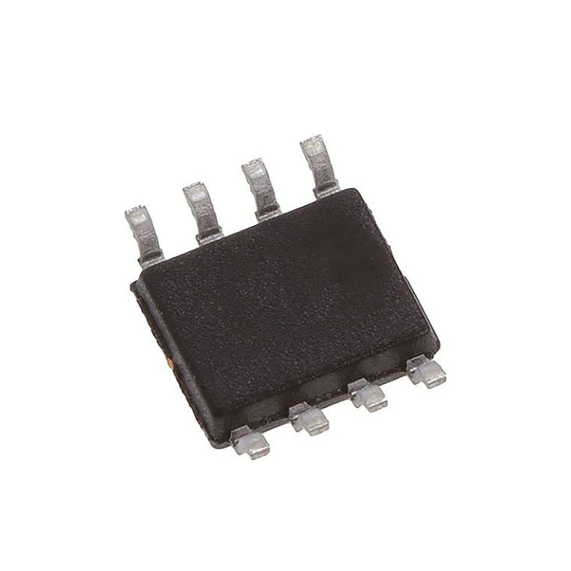
TLV840CADL28DBVR
Supervisory Circuits Low-voltage supervisor with adjustable-reset time delay and manual reset 5-SOT-23 -40 to 125


Brands: TEXAS INSTRUMENTS INC
Mfr.Part #: TLV840CADL28DBVR
Datasheet: TLV840CADL28DBVR Datasheet (PDF)
Package/Case: SOT-23-5
Product Type: Supervisory Circuits
RoHS Status:
Stock Condition: 6385 pcs, New Original
Warranty: 1 Year Ovaga Warranty - Find Out More
0
1
Add To BomTLV840CADL28DBVR General Description
The TLV840 family of voltage supervisors or reset ICs can operate at high voltage levels while maintaining very low quiescent current across the whole VDD and temperature range. TLV840 offers best combination of low power consumption, high accuracy and low propagation delay (tp_HL= 30 µs typical).
Reset output signal is asserted when the voltage at VDD drops below the negative voltage threshold (VIT-). Reset signal is cleared when VDD rise above VIT- plus hysteresis (VHYS) and the reset time delay (tD) expires. Reset time delay can be programmed by connecting a capacitor between the CT pin and ground for TLV840C and TLV840M. For a minimum reset delay time the CT pin can be left floating. TLV840N does not offer a programmable delay and offers fixed reset delay timing options: 40 µs, 2 ms, 10 ms, 30 ms, 50 ms, 80 ms, 100 ms, 150 ms, 200 ms.
Additional features: Low power-on reset voltage (VPOR), built-in glitch immunity protection for VDD, built-in hysteresis, low open-drain output leakage current (Ilkg(OD)). TLV840 is a perfect voltage monitoring solution for industrial applications and battery-powered / low-power applications.
Features
- Operating voltage range : 0.7 V to 6 V
- Nano supply current : 120 nA (Typical)
- Fixed threshold voltage (VIT-): 0.8 V to 5.4 V
- Threshold voltages available in 100mV steps
- High accuracy: ±0.5% (Typical)
- Built-in hysteresis (VHYS): 5% (Typical)
- Reset time delay (tD): capacitor-based programmable (TLV840C, TLV840M)
- Minimum time delay: 40 µs (typical) without capacitor
- Active-low manual reset (MR) (TLV840M)
- Four output topologies:
- TLV840xxDL: open-drain, active-low (RESET)
- TLV840xxPL: push-pull, active-low (RESET)
- TLV840xxDH: open-drain, active-high (RESET)
- TLV840xxPH: push-pull, active-high (RESET)
- Wide temperature range: –40°C to +125°C
- Package: SOT23-5 (DBV)
Specifications
| Parameter | Value | Parameter | Value |
|---|---|---|---|
| Source Content uid | TLV840CADL28DBVR | Pbfree Code | Yes |
| Rohs Code | Yes | Part Life Cycle Code | Active |
| Ihs Manufacturer | TEXAS INSTRUMENTS INC | Package Description | LSSOP, TSOP5/6,.11,37 |
| Reach Compliance Code | compliant | ECCN Code | EAR99 |
| HTS Code | 8542.39.00.01 | Date Of Intro | 2020-09-27 |
| Samacsys Manufacturer | Texas Instruments | Adjustable Threshold | NO |
| Analog IC - Other Type | POWER SUPPLY SUPPORT CIRCUIT | JESD-30 Code | R-PDSO-G5 |
| JESD-609 Code | e4 | Length | 2.9 mm |
| Moisture Sensitivity Level | 1 | Number of Channels | 1 |
| Number of Functions | 1 | Number of Terminals | 5 |
| Operating Temperature-Max | 125 °C | Operating Temperature-Min | -40 °C |
| Package Body Material | PLASTIC/EPOXY | Package Code | LSSOP |
| Package Equivalence Code | TSOP5/6,.11,37 | Package Shape | RECTANGULAR |
| Package Style | SMALL OUTLINE, LOW PROFILE, SHRINK PITCH | Peak Reflow Temperature (Cel) | 260 |
| Seated Height-Max | 1.45 mm | Supply Current-Max (Isup) | 0.0012 mA |
| Supply Voltage-Max (Vsup) | 6 V | Supply Voltage-Min (Vsup) | 0.7 V |
| Supply Voltage-Nom (Vsup) | 1.5 V | Surface Mount | YES |
| Temperature Grade | AUTOMOTIVE | Terminal Finish | NICKEL PALLADIUM GOLD |
| Terminal Form | GULL WING | Terminal Pitch | 0.95 mm |
| Terminal Position | DUAL | Threshold Voltage-Nom | +2.8V |
| Time@Peak Reflow Temperature-Max (s) | 30 |
Shipping
| Shipping Type | Ship Fee | Lead Time | |
|---|---|---|---|
 |
DHL | $20.00-$40.00 (0.50 KG) | 2-5 days |
 |
Fedex | $20.00-$40.00 (0.50 KG) | 2-5 days |
 |
UPS | $20.00-$40.00 (0.50 KG) | 2-5 days |
 |
TNT | $20.00-$40.00 (0.50 KG) | 2-5 days |
 |
EMS | $20.00-$40.00 (0.50 KG) | 2-5 days |
 |
REGISTERED AIR MAIL | $20.00-$40.00 (0.50 KG) | 2-5 days |
Processing Time:Shipping fee depend on different zone and country.
Payment
| Terms of payment | Hand Fee | |
|---|---|---|
 |
Wire Transfer | charge US$30.00 banking fee. |
 |
Paypal | charge 4.0% service fee. |
 |
Credit Card | charge 3.5% service fee. |
 |
Western Union | charge US.00 banking fee. |
 |
Money Gram | charge US$0.00 banking fee. |
Guarantees
1.The electronic components you purchase include 365 Days Warranty, We guarantee product quality.
2.If some of the items you received aren't of perfect quality, we would resiponsibly arrange your refund or replacement. But the items must remain their orginal condition.
Packing
-

Step1 :Product
-

Step2 :Vacuum packaging
-

Step3 :Anti-static bag
-

Step4 :Individual packaging
-

Step5 :Packaging boxes
-

Step6 :bar-code shipping tag


All the products will packing in anti-staticbag. Ship with ESD antistatic protection.
Outside ESD packing’s lable will use ourcompany’s information: Part Mumber, Brand and Quantity.
We will inspect all the goods before shipment,ensure all the products at good condition and ensure the parts are new originalmatch datasheet.
After all the goods are ensure no problems afterpacking, we will packing safely and send by global express. It exhibitsexcellent puncture and tear resistance along with good seal integrity.


We provide high quality products, thoughtful service and after sale guarantee
-

We have rich products, can meet your various needs.
-

Minimum order quantity starts from 1pcs.
-

Lowest international shipping fee starts from $0.00
-

365 days quality guarantee for all products