Images are for reference only See Product Specifications
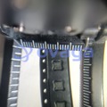
TI SN74AXC4T245PWR

Translation Transceiver 2 Element 2 Bit per Element 3-State Output 16-TSSOP


Brands: TI
Mfr.Part #: SN74AXC4T245PWR
Datasheet: SN74AXC4T245PWR Datasheet (PDF)
Package/Case: TSSOP-16
RoHS Status:
Stock Condition: 9500 pcs, New Original
Product Type: Standard Logic > Level Translator
Warranty: 1 Year Ovaga Warranty - Find Out More
0
1
*All prices are in USD
| Qty | Unit Price | Ext Price |
|---|---|---|
| 1 | $0.489 | $0.489 |
| 10 | $0.414 | $4.140 |
| 30 | $0.359 | $10.770 |
| 100 | $0.316 | $31.600 |
| 500 | $0.302 | $151.000 |
| 1000 | $0.293 | $293.000 |
In Stock:9500 PCS
SN74AXC4T245PWR General Description
The SN74AXC4T245 is a four-bit noninverting bus transceiver that uses two individually configurable power-supply rails. The device is operational with both VCCA and VCCB supplies as low as 0.65 V. The A port is designed to track VCCA, which accepts any supply voltage from 0.65 V to 3.6 V. The B port is designed to track VCCB, which also accepts any supply voltage from 0.65 V to 3.6 V. Additionally the SN74AXC4T245 is compatible with a single-supply system.
The SN74AXC4T245 device is designed for asynchronous communication between data buses. The device transmits data from the A bus to the B bus or from the B bus to the A bus, depending on the logic level of the direction-control inputs (1DIR and 2DIR). The output-enable inputs (1 OE and 2 OE) are used to disable the outputs so the buses are effectively isolated. The SN74AXC4T245 device is designed so the control pins (xDIR and x OE) are referenced to VCCA.
To ensure the high-impedance state of the level shifter I/Os during power up or power down, the x OE pins should be tied to VCCA through a pullup resistor.
This device is fully specified for partial-power-down applications using the Ioff current. The Ioff protection circuitry ensures that no excessive current is drawn from or to an input, output, or combined I/O that is biased to a specific voltage while the device is powered down.
The VCC isolation feature ensures that if either VCCA or VCCB is less than 100 mV, both I/O ports enter a high-impedance state by disabling their outputs.
Glitch-Free power supply sequencing allows either supply rail to be powered on or off in any order while providing robust power sequencing performance.
Features
- Fully Configurable Dual-Rail Design Allows Each Port to Operate With a Power Supply Range From 0.65 V to 3.6 V
- Operating Temperature From –40°C to +125°C
- Multiple Direction Control Pins to Allow Simultaneous Up and Down Translation
- Glitch-Free Power Supply Sequencing
- Up to 380 Mbps Support When Translating from 1.8 V to 3.3 V
- VCC Isolation Feature
- If Either VCC Input is Below 100 mV, All I/Os Outputs are Disabled and Become High-Impedance
- Ioff Supports Partial-Power-Down Mode Operation
- Compatible With AVC Family Level Shifters
- Latch-Up Performance Exceeds 100 mA Per JESD 78, Class II
- ESD Protection Exceeds JESD 22
- 8000-V Human-Body Model
- 1000-V Charged-Device Model
Specifications
| Parameter | Value | Parameter | Value |
|---|---|---|---|
| Technology family | AXC | Applications | JTAG, SPI, UART |
| Bits (#) | 4 | High input voltage (min) (V) | 0.455 |
| High input voltage (max) (V) | 3.6 | Vout (min) (V) | 0.65 |
| Vout (max) (V) | 3.6 | Data rate (max) (MBps) | 380 |
| IOH (max) (mA) | -12 | IOL (max) (mA) | 12 |
| Supply current (max) (µA) | 40 | Features | Output enable, Overvoltage tolerant inputs, Partial power down (Ioff), Vcc isolation |
| Input type | Standard CMOS | Output type | 3-State, Balanced CMOS, Push-Pull |
| Rating | Catalog |
Shipping
| Shipping Type | Ship Fee | Lead Time | |
|---|---|---|---|
 |
DHL | $20.00-$40.00 (0.50 KG) | 2-5 days |
 |
Fedex | $20.00-$40.00 (0.50 KG) | 2-5 days |
 |
UPS | $20.00-$40.00 (0.50 KG) | 2-5 days |
 |
TNT | $20.00-$40.00 (0.50 KG) | 2-5 days |
 |
EMS | $20.00-$40.00 (0.50 KG) | 2-5 days |
 |
REGISTERED AIR MAIL | $20.00-$40.00 (0.50 KG) | 2-5 days |
Processing Time:Shipping fee depend on different zone and country.
Payment
| Terms of payment | Hand Fee | |
|---|---|---|
 |
Wire Transfer | charge US$30.00 banking fee. |
 |
Paypal | charge 4.0% service fee. |
 |
Credit Card | charge 3.5% service fee. |
 |
Western Union | charge US.00 banking fee. |
 |
Money Gram | charge US$0.00 banking fee. |
Guarantees
1.The electronic components you purchase include 365 Days Warranty, We guarantee product quality.
2.If some of the items you received aren't of perfect quality, we would resiponsibly arrange your refund or replacement. But the items must remain their orginal condition.
Packing
-

Step1 :Product
-

Step2 :Vacuum packaging
-

Step3 :Anti-static bag
-

Step4 :Individual packaging
-

Step5 :Packaging boxes
-

Step6 :bar-code shipping tag


All the products will packing in anti-staticbag. Ship with ESD antistatic protection.
Outside ESD packing’s lable will use ourcompany’s information: Part Mumber, Brand and Quantity.
We will inspect all the goods before shipment,ensure all the products at good condition and ensure the parts are new originalmatch datasheet.
After all the goods are ensure no problems afterpacking, we will packing safely and send by global express. It exhibitsexcellent puncture and tear resistance along with good seal integrity.


We provide high quality products, thoughtful service and after sale guarantee
-

We have rich products, can meet your various needs.
-

Minimum order quantity starts from 1pcs.
-

Lowest international shipping fee starts from $0.00
-

365 days quality guarantee for all products