Images are for reference only See Product Specifications
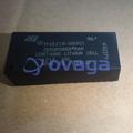
K524G2GACB-A050
DDR DRAM, 64MX16, 5.5ns, CMOS, PBGA137, 10.5 X 13 MM, 1.2 MM HEIGHT, 0.80 MM PITCH, FBGA-137


Brands: SAMSUNG
Mfr.Part #: K524G2GACB-A050
Datasheet: K524G2GACB-A050 Datasheet (PDF)
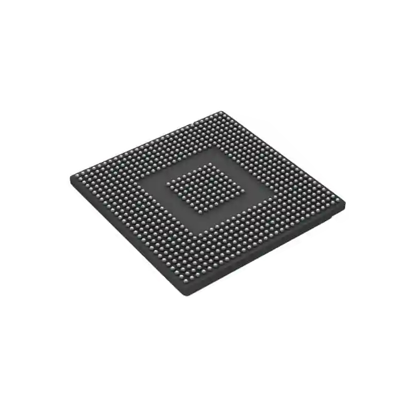
Package/Case: BGA
Product Type: Memory chips
RoHS Status:
Stock Condition: 6284 pcs, New Original
Warranty: 1 Year Ovaga Warranty - Find Out More
0
1
Add To BomK524G2GACB-A050 General Description
GENERAL DESCRIPTION The K524G2GACB is a Multi Chip Package Memory which combines 4Gbit NAND Flash Memory an 2Gbit DDR synchronous high data rate Dynamic RAM. NAND cell provides the most cost-effective solution for the solid state application market. A program operation can be performed in typical 250µs on the (1K+32)Word page and an erase operation can be performed in typical 2ms on a (64K+2K)Word block. Data in the data register can be read out at 42ns cycle time per Word. The I/O pins serve as the ports for address and data input/output as well as command input. The on-chip write controller automates all program and erase functions including pulse repetition, where required, and internal verification and margining of data. Even the write-intensive systems can take advantage of the device′s extended reliability of 100K program/erase cycles by providing ECC(Error Correcting Code) with real time mapping-out algorithm. The device is an optimum solution for large nonvolatile storage applications such as solid state file storage and other portable applications requiring non-volatility. In 2Gbit Mobile DDR, Synchronous design make a device controlled precisely with the use of system clock. Range of operating frequencies, programmable burst length and programmable latencies allow the same device to be useful for a variety of high bandwidth, high performance memory system applications.FEATURES• Operating Temperature : -25°C ~ 85°C • Package : 137-ball FBGA Type - 10.5 x 13 x 1.2mmt, 0.8mm pitch • Voltage Supply : 1.7V ~ 1.95V • Organization - Memory Cell Array : (256M + 8M) x 16bit for 4Gb (512M + 16M) x 16bit for 8Gb DDP - Data Register : (1K + 32) x 16bit • Automatic Program and Erase - Page Program : (1K + 32)Word - Block Erase : (64K + 2K)Word • Page Read Operation - Page Size : (1K + 32)Word - Random Read : 40µs(Max.) - Serial Access : 42ns(Min.) • Fast Write Cycle Time - Page Program time : 250µs(Typ.) - Block Erase Time : 2ms(Typ.) • Command/Address/Data Multiplexed I/O Port • Hardware Data - Program/Erase Lockout During Power Transitions • Reliable CMOS Floating-Gate Technology -Endurance : 100K Program/Erase Cycles with 1bit/256Word ECC for x16 • Command Driven Operation • Unique ID for Copyright Protection • VDD/VDDQ = 1.8V/1.8V • Double-data-rate architecture; two data transfers per clock cycle • Bidirectional data strobe(DQS) • Four banks operation • Differential clock inputs(CK and CK) • MRS cycle with address key programs - CAS Latency ( 3 ) - Burst Length ( 2, 4, 8, 16 ) - Burst Type (Sequential & Interleave) • EMRS cycle with address key programs - Partial Array Self Refresh ( Full, 1/2, 1/4 Array ) - Output Driver Strength Control ( Full, 1/2, 1/4, 1/8, 3/4, 3/8, 5/8, 7/8 ) • Internal Temperature Compensated Self Refresh • All inputs except data & DM are sampled at the positive going edge of the system clock(CK). • Data I/O transactions on both edges of data strobe, DM for masking. • Edge aligned data output, center aligned data input. • No DLL; CK to DQS is not synchronized. • DM0 - DM3 for write masking only. • Auto refresh duty cycle - 7.8us • Clock stop capability
Features
- Operating Temperature : -25°C ~ 85°C
- Package : 137-ball FBGA Type - 10.5 x 13 x 1.2mmt, 0.8mm pitch
Specifications
| Parameter | Value | Parameter | Value |
|---|---|---|---|
| Manufacturer | SAMSUNG |
Shipping
| Shipping Type | Ship Fee | Lead Time | |
|---|---|---|---|
 |
DHL | $20.00-$40.00 (0.50 KG) | 2-5 days |
 |
Fedex | $20.00-$40.00 (0.50 KG) | 2-5 days |
 |
UPS | $20.00-$40.00 (0.50 KG) | 2-5 days |
 |
TNT | $20.00-$40.00 (0.50 KG) | 2-5 days |
 |
EMS | $20.00-$40.00 (0.50 KG) | 2-5 days |
 |
REGISTERED AIR MAIL | $20.00-$40.00 (0.50 KG) | 2-5 days |
Processing Time:Shipping fee depend on different zone and country.
Payment
| Terms of payment | Hand Fee | |
|---|---|---|
 |
Wire Transfer | charge US$30.00 banking fee. |
 |
Paypal | charge 4.0% service fee. |
 |
Credit Card | charge 3.5% service fee. |
 |
Western Union | charge US.00 banking fee. |
 |
Money Gram | charge US$0.00 banking fee. |
Guarantees
1.The electronic components you purchase include 365 Days Warranty, We guarantee product quality.
2.If some of the items you received aren't of perfect quality, we would resiponsibly arrange your refund or replacement. But the items must remain their orginal condition.
Packing
-

Step1 :Product
-

Step2 :Vacuum packaging
-

Step3 :Anti-static bag
-

Step4 :Individual packaging
-

Step5 :Packaging boxes
-

Step6 :bar-code shipping tag


All the products will packing in anti-staticbag. Ship with ESD antistatic protection.
Outside ESD packing’s lable will use ourcompany’s information: Part Mumber, Brand and Quantity.
We will inspect all the goods before shipment,ensure all the products at good condition and ensure the parts are new originalmatch datasheet.
After all the goods are ensure no problems afterpacking, we will packing safely and send by global express. It exhibitsexcellent puncture and tear resistance along with good seal integrity.


We provide high quality products, thoughtful service and after sale guarantee
-

We have rich products, can meet your various needs.
-

Minimum order quantity starts from 1pcs.
-

Lowest international shipping fee starts from $0.00
-

365 days quality guarantee for all products