Images are for reference only See Product Specifications
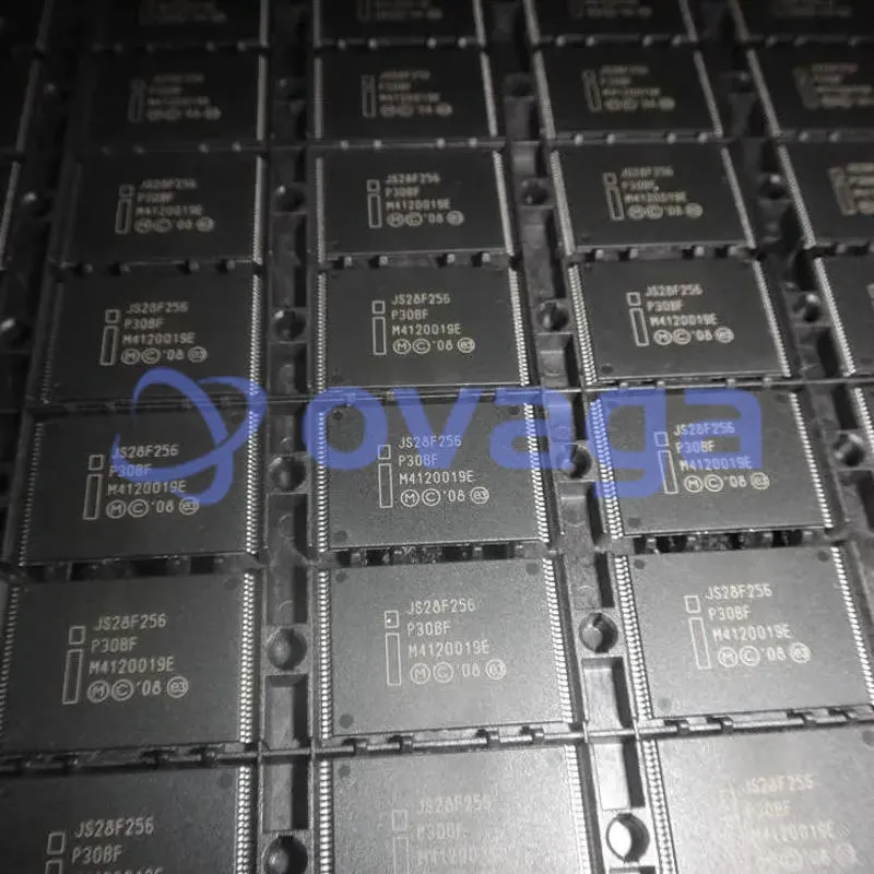
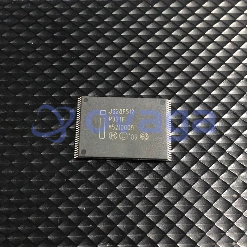
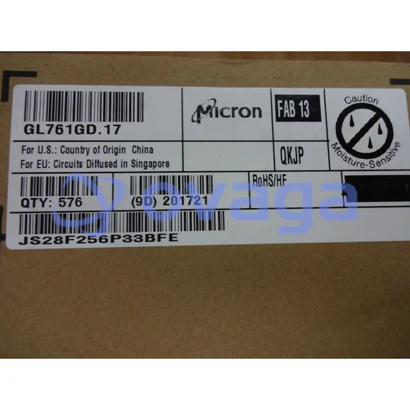
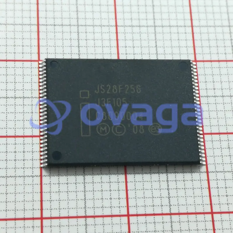
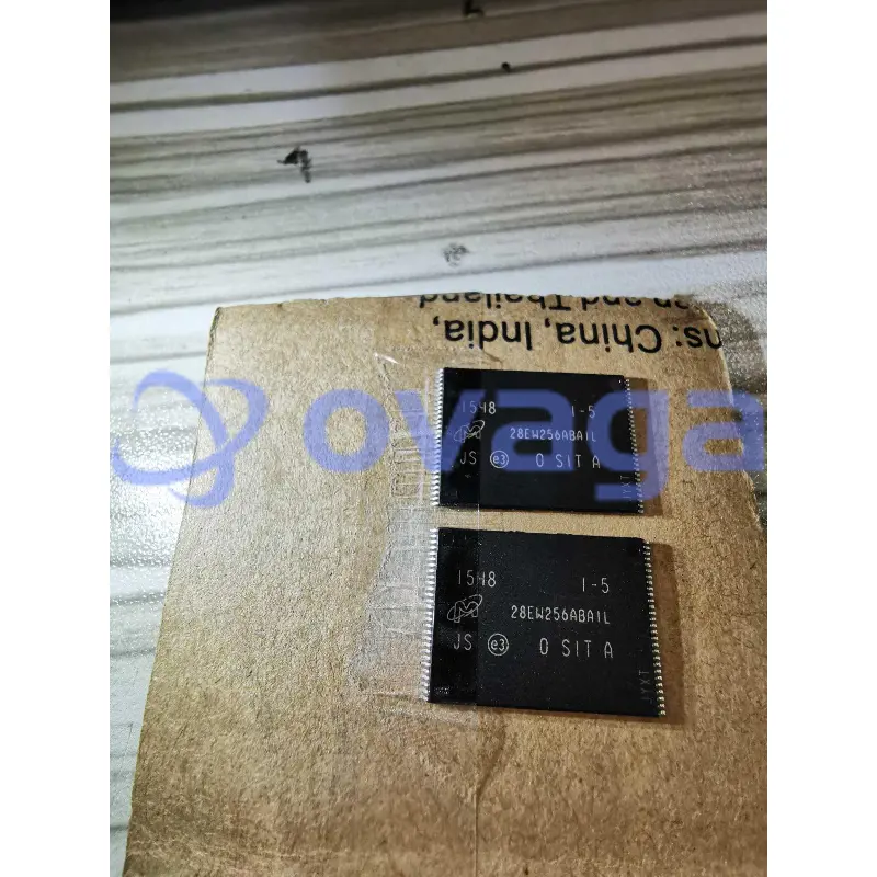
JS28F256P30BFE
NOR Flash Parallel 256Mbit 16 56/56


Brands: MICRON TECHNOLOGY INC
Mfr.Part #: JS28F256P30BFE
Datasheet: JS28F256P30BFE Datasheet (PDF)
Package/Case: TSOP-56
Product Type: NOR Flash
Features
- High performance
- — 85/88 ns initial access
- — 40 MHz with zero wait states, 20 ns clock-to data output synchronous-burst read mode
- — 25 ns asynchronous-page read mode
- — 4-, 8-, 16-, and continuous-word burst mode
- — Buffered Enhanced Factory Programming (BEFP) at 5 µs/byte (Typ)
- — 1.8 V buffered programming at 7 µs/byte (Typ)
- Architecture
- — Multi-Level Cell Technology: Highest Density at Lowest Cost
- — Asymmetrically-blocked architecture
- — Four 32-KByte parameter blocks: top or bottom configuration
- — 128-KByte main blocks
- Voltage and Power
- —VCC(core) voltage: 1.7 V – 2.0 V
- —VCCQ (I/O) voltage: 1.7 V – 3.6 V
- — Standby current: 55 µA (Typ) for 256-Mbit
- — 4-Word synchronous read current: 13 mA (Typ) at 40 MHz
- Quality and Reliability
- — Operating temperature: –40 °C to +85 °C
- 1-Gbit in SCSP is –30 °C to +85 °C
- — Minimum 100,000 erase cycles per block
- — ETOX™ VIII process technology (130 nm)
- Security
- — One-Time Programmable Registers:
- 64 unique factory device identifier bits
- 64 user-programmable OTP bits
- Additional 2048 user-programmable OTP bits
- — Selectable OTP Space in Main Array:
- 4x32KB parameter blocks + 3x128KB main blocks (top or bottom configuration)
- — Absolute write protection: VPP= VSS
- — Power-transition erase/program lockout
- — Individual zero-latency block locking
- — Individual block lock-down
- Software
- — 20 µs (Typ) program suspend
- — 20 µs (Typ) erase suspend
- —Intel® Flash Data Integrator optimized
- — Basic Command Set and Extended Command Set compatible
- — Common Flash Interface capable
- Density and Packaging
- — 64/128/256-Mbit densities in 56-Lead TSOP package
- — 64/128/256/512-Mbit densities in 64-Ball Intel®Easy BGA package
- — 64/128/256/512-Mbit and 1-Gbit densities in Intel®QUAD+ SCSP
- — 16-bit wide data bus
Specifications
| Parameter | Value | Parameter | Value |
|---|---|---|---|
| Pbfree Code | Yes | Rohs Code | Yes |
| Part Life Cycle Code | Obsolete | Ihs Manufacturer | MICRON TECHNOLOGY INC |
| Package Description | TSOP-56 | Reach Compliance Code | compliant |
| ECCN Code | EAR99 | HTS Code | 8542.32.00.51 |
| Samacsys Manufacturer | Micron | Access Time-Max | 20 ns |
| Additional Feature | IT ALSO HAVE ASYNCHRONOUS OPERATING MODE | Boot Block | BOTTOM |
| Command User Interface | YES | Common Flash Interface | YES |
| Data Polling | NO | JESD-30 Code | R-PDSO-G56 |
| JESD-609 Code | e3 | Length | 18.4 mm |
| Memory Density | 268435456 bit | Memory IC Type | FLASH |
| Memory Width | 16 | Number of Functions | 1 |
| Number of Sectors/Size | 4,255 | Number of Terminals | 56 |
| Number of Words | 16777216 words | Number of Words Code | 16000000 |
| Operating Mode | SYNCHRONOUS | Operating Temperature-Max | 85 °C |
| Operating Temperature-Min | -40 °C | Organization | 16MX16 |
| Package Body Material | PLASTIC/EPOXY | Package Code | TSSOP |
| Package Equivalence Code | TSSOP56,.8,20 | Package Shape | RECTANGULAR |
| Package Style | SMALL OUTLINE, THIN PROFILE, SHRINK PITCH | Parallel/Serial | PARALLEL |
| Programming Voltage | 1.8 V | Qualification Status | Not Qualified |
| Seated Height-Max | 1.025 mm | Sector Size | 16K,64K |
| Standby Current-Max | 0.00021 A | Supply Current-Max | 0.031 mA |
| Supply Voltage-Max (Vsup) | 2 V | Supply Voltage-Min (Vsup) | 1.7 V |
| Supply Voltage-Nom (Vsup) | 1.8 V | Surface Mount | YES |
| Technology | CMOS | Temperature Grade | INDUSTRIAL |
| Terminal Finish | MATTE TIN | Terminal Form | GULL WING |
| Terminal Pitch | 0.5 mm | Terminal Position | DUAL |
| Toggle Bit | NO | Type | NOR TYPE |
| Width | 14 mm |
Shipping
| Shipping Type | Ship Fee | Lead Time | |
|---|---|---|---|
 |
DHL | $20.00-$40.00 (0.50 KG) | 2-5 days |
 |
Fedex | $20.00-$40.00 (0.50 KG) | 2-5 days |
 |
UPS | $20.00-$40.00 (0.50 KG) | 2-5 days |
 |
TNT | $20.00-$40.00 (0.50 KG) | 2-5 days |
 |
EMS | $20.00-$40.00 (0.50 KG) | 2-5 days |
 |
REGISTERED AIR MAIL | $20.00-$40.00 (0.50 KG) | 2-5 days |
Processing Time:Shipping fee depend on different zone and country.
Payment
| Terms of payment | Hand Fee | |
|---|---|---|
 |
Wire Transfer | charge US$30.00 banking fee. |
 |
Paypal | charge 4.0% service fee. |
 |
Credit Card | charge 3.5% service fee. |
 |
Western Union | charge US.00 banking fee. |
 |
Money Gram | charge US$0.00 banking fee. |
Guarantees
1.The electronic components you purchase include 365 Days Warranty, We guarantee product quality.
2.If some of the items you received aren't of perfect quality, we would resiponsibly arrange your refund or replacement. But the items must remain their orginal condition.
Packing
-

Step1 :Product
-

Step2 :Vacuum packaging
-

Step3 :Anti-static bag
-

Step4 :Individual packaging
-

Step5 :Packaging boxes
-

Step6 :bar-code shipping tag
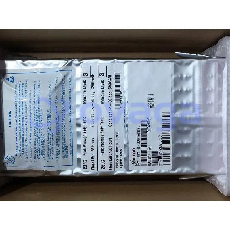
All the products will packing in anti-staticbag. Ship with ESD antistatic protection.
Outside ESD packing’s lable will use ourcompany’s information: Part Mumber, Brand and Quantity.
We will inspect all the goods before shipment,ensure all the products at good condition and ensure the parts are new originalmatch datasheet.
After all the goods are ensure no problems afterpacking, we will packing safely and send by global express. It exhibitsexcellent puncture and tear resistance along with good seal integrity.


Part points
-
The JS28F256P30BFE is a flash memory chip manufactured by Intel. It offers 256 megabits of storage capacity and uses a parallel interface. With fast read and program speeds, it's commonly used in embedded systems, consumer electronics, and industrial applications for data storage and firmware updates.
-
Equivalent
Equivalent products to the JS28F256P30BFE chip include the Intel 28F256P30B, SST28SF256P30B, and AM28F256P30BF. These chips share similar specifications and functionalities, making them suitable alternatives for various applications. -
Features
1. 256Mb NAND Flash Memory 2. 3.0V Supply Voltage 3. Extended Temperature Range: -40°C to 85°C 4. Small Form Factor: 48-ball FBGA 5. High Speed Interface: 50ns Page Access Time 6. Flexible Erase and Program Algorithms 7. Data Retention: 20 Years 8. Industry-Standard JEDEC Packaging -
Pinout
The JS28F256P30BFE is a 256-megabit (32 megabyte) flash memory chip. It has a 64-pin count. The pins serve functions such as power supply, address input/output, data input/output, and control signals for reading, writing, and erasing data. -
Manufacturer
The JS28F256P30BFE is manufactured by Intel Corporation, a leading American multinational corporation known for designing and manufacturing semiconductor chips and related products. Intel is one of the largest and most influential technology companies globally, particularly renowned for its microprocessors for personal computers. -
Application Field
The JS28F256P30BFE is commonly used in embedded systems, telecommunications equipment, networking devices, and automotive electronics for storing firmware, boot code, and data. It's suitable for applications requiring reliable, high-density, non-volatile memory with fast read and write operations. -
Package
The JS28F256P30BFE chip is a BGA package type, with a TSOP form factor, and a size of 49.21 mm x 25.61 mm.
We provide high quality products, thoughtful service and after sale guarantee
-

We have rich products, can meet your various needs.
-

Minimum order quantity starts from 1pcs.
-

Lowest international shipping fee starts from $0.00
-

365 days quality guarantee for all products
Recommend
-
-
-
-
-
Infineon Technologies Corporation
NOR Flash Parallel 3V/3.3V 64M-bit 8M x 8/4M x 16 ...
-