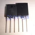
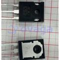
Images are for reference only See Product Specifications
FQT3P20TF

P-Channel 200 V 670mA (Tc) 2.5W (Tc) Surface Mount SOT-223-4


Brands: ONSEMI
Mfr.Part #: FQT3P20TF
Datasheet: FQT3P20TF Datasheet (PDF)
Package/Case: SOT-223-4
RoHS Status:
Stock Condition: 5625 pcs, New Original
Product Type: MOSFET
Warranty: 1 Year Ovaga Warranty - Find Out More
0
1
*All prices are in USD
| Qty | Unit Price | Ext Price |
|---|---|---|
| 1 | $0.862 | $0.862 |
| 10 | $0.727 | $7.270 |
| 30 | $0.659 | $19.770 |
| 100 | $0.591 | $59.100 |
| 500 | $0.552 | $276.000 |
| 1000 | $0.531 | $531.000 |
In Stock:5625 PCS
FQT3P20TF General Description
This P-Channel enhancement mode power MOSFET is produced using ON Semiconductor Semiconductor’s proprietary planar stripe and DMOS technology. This advanced MOSFET technology has been especially tailored to reduce on-state resistance, and to provide superior switching performance and high avalanche energy strength. These devices are suitable for switched mode power supplies, audio amplifier, DC motor control, and variable switching power applications.
Features
- -0.67A, -200V, RDS(on) = 2.7Ω(Max.) @VGS = -10 V, ID = -0.335A
- Low gate charge ( Typ. 6nC)
- Low Crss ( Typ. 7.5pF)
Application
- Other Industrial
Specifications
| Parameter | Value | Parameter | Value |
|---|---|---|---|
| Source Content uid | FQT3P20TF | Pbfree Code | Yes |
| Part Life Cycle Code | Lifetime Buy | Ihs Manufacturer | ONSEMI |
| Manufacturer Package Code | 318H-01 | Reach Compliance Code | not_compliant |
| ECCN Code | EAR99 | Factory Lead Time | 16 Weeks |
| Samacsys Manufacturer | onsemi | Avalanche Energy Rating (Eas) | 150 mJ |
| Case Connection | DRAIN | Configuration | SINGLE WITH BUILT-IN DIODE |
| DS Breakdown Voltage-Min | 200 V | Drain Current-Max (ID) | 0.67 A |
| Drain-source On Resistance-Max | 2.7 Ω | FET Technology | METAL-OXIDE SEMICONDUCTOR |
| JESD-30 Code | R-PDSO-G4 | JESD-609 Code | e3 |
| Moisture Sensitivity Level | 1 | Number of Elements | 1 |
| Number of Terminals | 4 | Operating Mode | ENHANCEMENT MODE |
| Operating Temperature-Max | 150 °C | Package Body Material | PLASTIC/EPOXY |
| Package Shape | RECTANGULAR | Package Style | SMALL OUTLINE |
| Peak Reflow Temperature (Cel) | 260 | Polarity/Channel Type | P-CHANNEL |
| Power Dissipation-Max (Abs) | 2.5 W | Pulsed Drain Current-Max (IDM) | 2.7 A |
| Qualification Status | Not Qualified | Surface Mount | YES |
| Terminal Finish | MATTE TIN | Terminal Form | GULL WING |
| Terminal Position | DUAL | Time@Peak Reflow Temperature-Max (s) | 30 |
| Transistor Application | SWITCHING |
Shipping
| Shipping Type | Ship Fee | Lead Time | |
|---|---|---|---|
 |
DHL | $20.00-$40.00 (0.50 KG) | 2-5 days |
 |
Fedex | $20.00-$40.00 (0.50 KG) | 2-5 days |
 |
UPS | $20.00-$40.00 (0.50 KG) | 2-5 days |
 |
TNT | $20.00-$40.00 (0.50 KG) | 2-5 days |
 |
EMS | $20.00-$40.00 (0.50 KG) | 2-5 days |
 |
REGISTERED AIR MAIL | $20.00-$40.00 (0.50 KG) | 2-5 days |
Processing Time:Shipping fee depend on different zone and country.
Payment
| Terms of payment | Hand Fee | |
|---|---|---|
 |
Wire Transfer | charge US$30.00 banking fee. |
 |
Paypal | charge 4.0% service fee. |
 |
Credit Card | charge 3.5% service fee. |
 |
Western Union | charge US.00 banking fee. |
 |
Money Gram | charge US$0.00 banking fee. |
Guarantees
1.The electronic components you purchase include 365 Days Warranty, We guarantee product quality.
2.If some of the items you received aren't of perfect quality, we would resiponsibly arrange your refund or replacement. But the items must remain their orginal condition.
Packing
-

Step1 :Product
-

Step2 :Vacuum packaging
-

Step3 :Anti-static bag
-

Step4 :Individual packaging
-

Step5 :Packaging boxes
-

Step6 :bar-code shipping tag


All the products will packing in anti-staticbag. Ship with ESD antistatic protection.
Outside ESD packing’s lable will use ourcompany’s information: Part Mumber, Brand and Quantity.
We will inspect all the goods before shipment,ensure all the products at good condition and ensure the parts are new originalmatch datasheet.
After all the goods are ensure no problems afterpacking, we will packing safely and send by global express. It exhibitsexcellent puncture and tear resistance along with good seal integrity.


Part points
-
The FQT3P20TF chip is a power MOSFET device designed to control current flow in electronic circuits. It features a low on-resistance and high switching speed, making it suitable for various applications, including power management and motor control. This chip is commonly used in automotive and industrial sectors, where efficient power control is essential.
-
Features
The FQT3P20TF is a high-voltage N-channel MOSFET with a low on-resistance and low gate charge. It is designed for applications requiring high efficiency and compact designs. With its advanced features, it offers improved power handling, high-speed switching, and enhanced thermal performance. -
Pinout
The FQT3P20TF is a 20-pin power MOSFET transistor with three P-channel enhancement-mode transistors. Its pin count and function are specific to its packaging and manufacturer, and may vary. Please refer to the datasheet or manufacturer's documentation for detailed information. -
Manufacturer
The manufacturer of the FQT3P20TF is ON Semiconductor. It is a global semiconductor company that designs and produces a wide range of innovative power and signal management, logic, and discrete devices for various industries including automotive, communications, computing, industrial, medical, and consumer. -
Application Field
The FQT3P20TF is a power field-effect transistor (FET) specifically designed for high-frequency applications. It can be used in various applications including RF amplification, small signal switching, and other high-speed switching applications. -
Package
The FQT3P20TF chip is packaged in a TO-220F form factor, which is a through-hole package commonly used for high power applications. The size of the chip package is approximately 10.16mm x 15.87mm x 4.8mm (0.4" x 0.625" x 0.189").


We provide high quality products, thoughtful service and after sale guarantee
-

We have rich products, can meet your various needs.
-

Minimum order quantity starts from 1pcs.
-

Lowest international shipping fee starts from $0.00
-

365 days quality guarantee for all products