


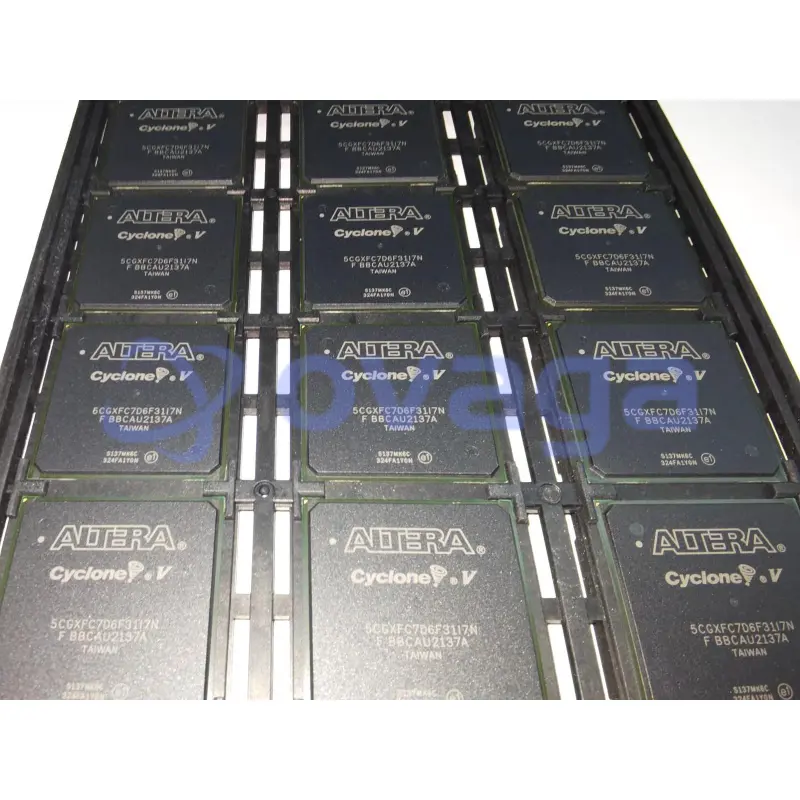
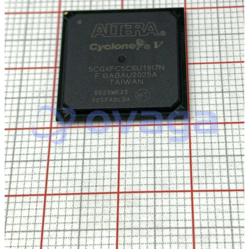
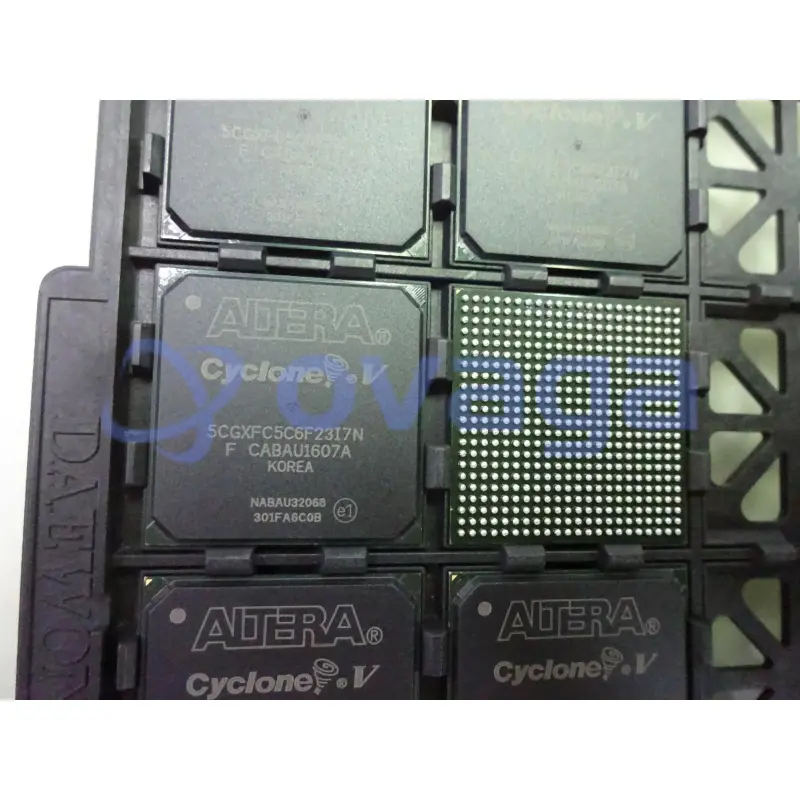
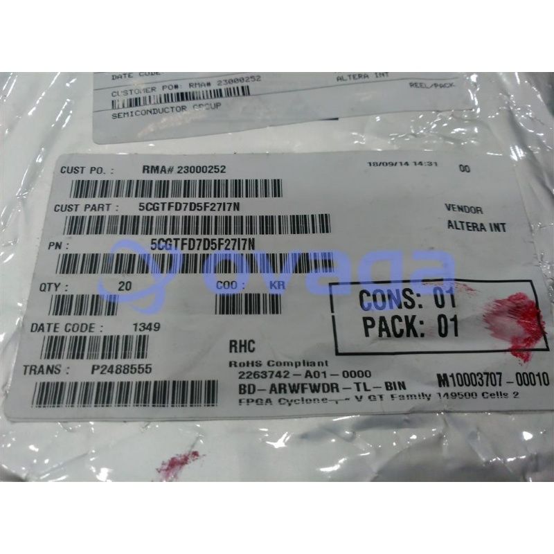
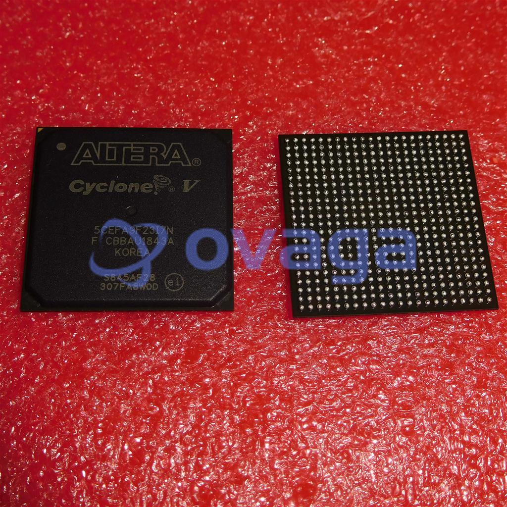
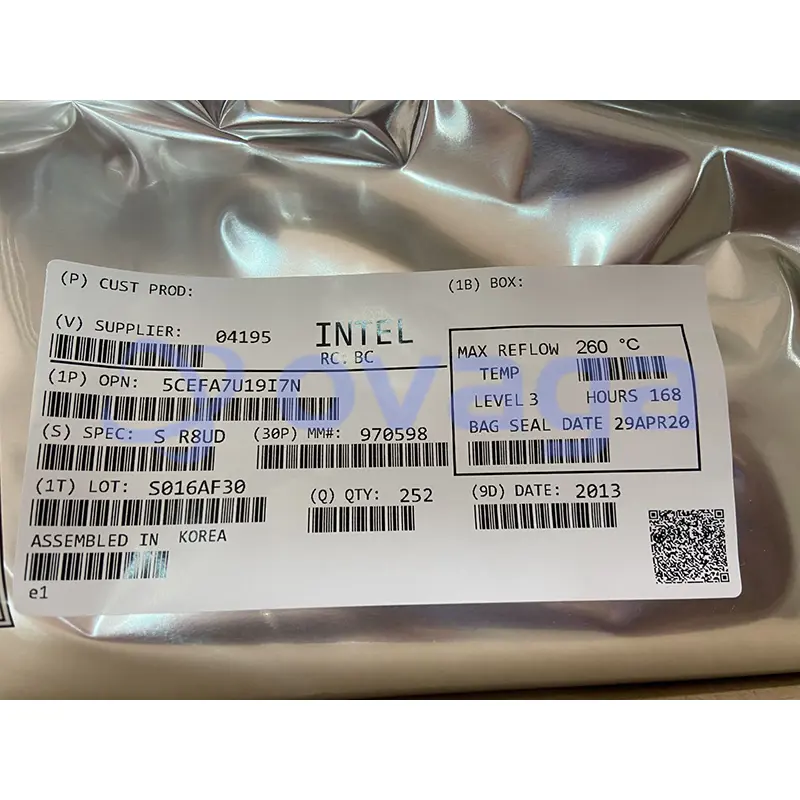
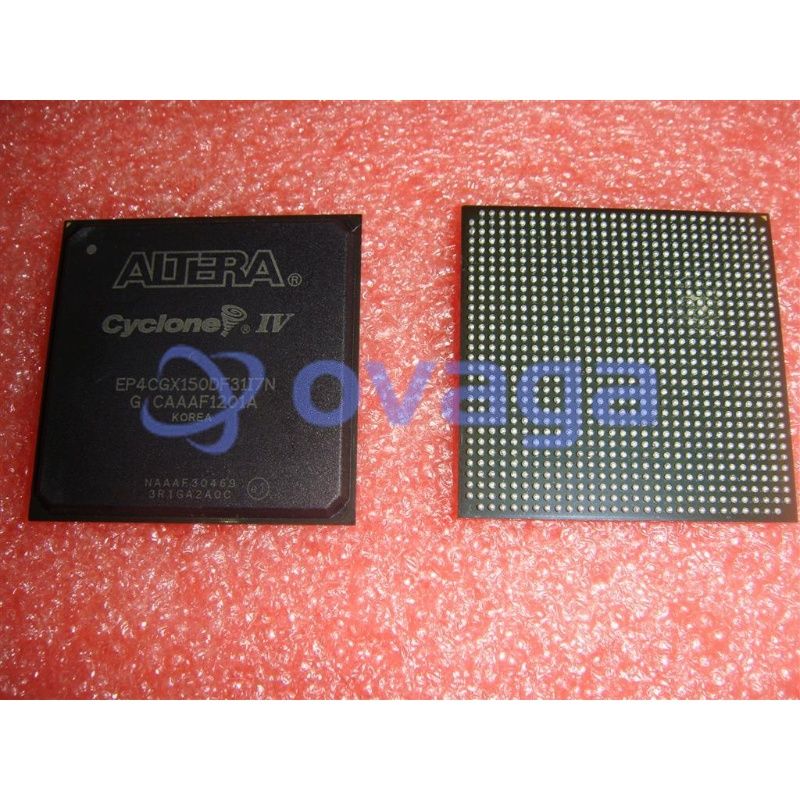
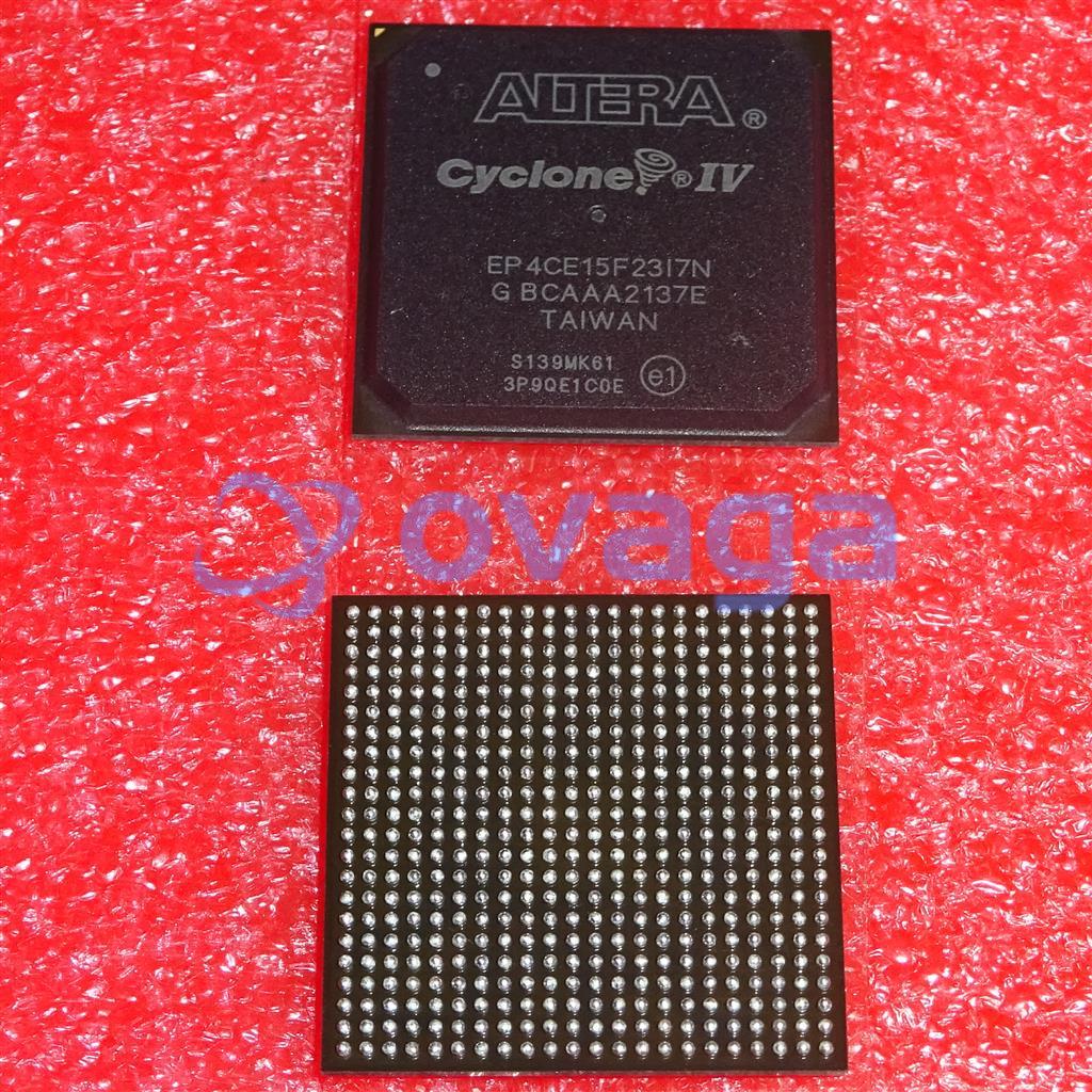
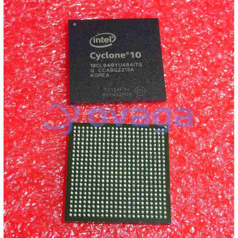
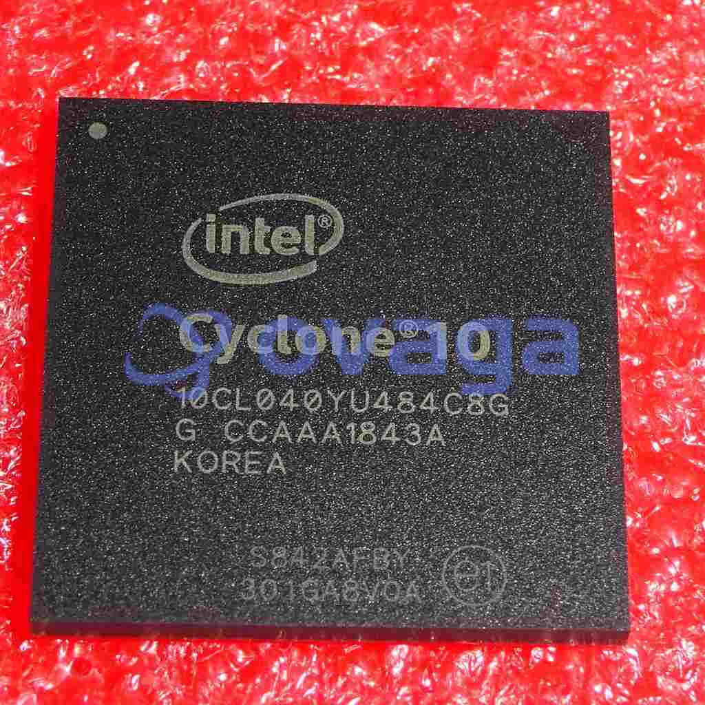
Images are for reference only See Product Specifications
Intel 5CGXFC7C6U19I7N
FPGA Cyclone® V GX Family 149500 Cells 28nm Technology 1.1V 484-Pin UFBGA


Brands: Intel Corp
Mfr.Part #: 5CGXFC7C6U19I7N
Datasheet: 5CGXFC7C6U19I7N Datasheet (PDF)
Package/Case: BGA-484
Product Type: Programmable Logic ICs
5CGXFC7C6U19I7N General Description
Cyclone® V GX Field Programmable Gate Array (FPGA) IC 240 7880704 149500 484-FBGA

Specifications
| Parameter | Value | Parameter | Value |
|---|---|---|---|
| feature-family-name | Cyclone® V GX | feature-process-technology | 28nm |
| feature-maximum-number-of-user-i-os | 240 | feature-number-of-registers | 225920 |
| feature-device-logic-cells | 149500 | feature-device-system-gates | |
| feature-number-of-multipliers | 312 (18x18) | feature-program-memory-type | SRAM |
| feature-ram-bits-kbit | 6860 | feature-total-number-of-block-ram | 686 |
| feature-ethernet-macs | 2 | feature-supported-ip-core | |
| feature-supported-ip-core-manufacture | feature-maximum-number-of-serdes-channels | ||
| feature-device-logic-units | 149500 | feature-device-number-of-dlls-plls | 7 |
| feature-transceiver-blocks | 9 | feature-transceiver-speed-gbps | 3.125 |
| feature-dedicated-dsp | 156 | feature-pci-blocks | 2 |
| feature-programmability | Yes | feature-maximum-internal-frequency-mhz | |
| feature-speed-grade | 7 | feature-giga-multiply-accumulates-per-second | |
| feature-differential-i-o-standards-supported | LVPECL|LVDS | feature-single-ended-i-o-standards-supported | LVTTL|LVCMOS |
| feature-external-memory-interface | DDR2 SDRAM|DDR3 SDRAM|LPDDR2 | feature-minimum-operating-supply-voltage-v | 1.07 |
| feature-maximum-operating-supply-voltage-v | 1.13 | feature-packaging | |
| feature-rohs | feature-rad-hard | ||
| feature-pin-count | 484 | feature-supplier-package | UFBGA |
| feature-standard-package-name1 | BGA | feature-cecc-qualified | No |
| feature-esd-protection | feature-escc-qualified | ||
| feature-military | No | feature-aec-qualified | No |
| feature-aec-qualified-number | feature-auto-motive | No | |
| feature-p-pap | No | feature-eccn-code | 3A991 |
| feature-svhc | Yes |
Shipping
| Shipping Type | Ship Fee | Lead Time | |
|---|---|---|---|
 |
DHL | $20.00-$40.00 (0.50 KG) | 2-5 days |
 |
Fedex | $20.00-$40.00 (0.50 KG) | 2-5 days |
 |
UPS | $20.00-$40.00 (0.50 KG) | 2-5 days |
 |
TNT | $20.00-$40.00 (0.50 KG) | 2-5 days |
 |
EMS | $20.00-$40.00 (0.50 KG) | 2-5 days |
 |
REGISTERED AIR MAIL | $20.00-$40.00 (0.50 KG) | 2-5 days |
Processing Time:Shipping fee depend on different zone and country.
Payment
| Terms of payment | Hand Fee | |
|---|---|---|
 |
Wire Transfer | charge US$30.00 banking fee. |
 |
Paypal | charge 4.0% service fee. |
 |
Credit Card | charge 3.5% service fee. |
 |
Western Union | charge US.00 banking fee. |
 |
Money Gram | charge US$0.00 banking fee. |
Guarantees
1.The electronic components you purchase include 365 Days Warranty, We guarantee product quality.
2.If some of the items you received aren't of perfect quality, we would resiponsibly arrange your refund or replacement. But the items must remain their orginal condition.
Packing
-

Step1 :Product
-

Step2 :Vacuum packaging
-

Step3 :Anti-static bag
-

Step4 :Individual packaging
-

Step5 :Packaging boxes
-

Step6 :bar-code shipping tag
All the products will packing in anti-staticbag. Ship with ESD antistatic protection.
Outside ESD packing’s lable will use ourcompany’s information: Part Mumber, Brand and Quantity.
We will inspect all the goods before shipment,ensure all the products at good condition and ensure the parts are new originalmatch datasheet.
After all the goods are ensure no problems afterpacking, we will packing safely and send by global express. It exhibitsexcellent puncture and tear resistance along with good seal integrity.


Part points
-
The 5CGXFC7C6U19I7N chip is a high-performance and energy-efficient field-programmable gate array (FPGA) positioned in Intel's Cyclone V GX series. It offers versatile features like high-speed transceivers, embedded memory, and digital signal processing capabilities. This chip is commonly used in various applications such as industrial automation, automotive systems, and telecommunications among others.
-
Features
The main features of 5CGXFC7C6U19I7N include a Cyclone V FPGA technology, 6,272 Logic Elements, 620 I/O pins, 414 user I/Os and 360Kb of Embedded Memory. It also offers various interfaces like PCIe, Ethernet, and USB, making it suitable for a wide range of applications. -
Pinout
The 5CGXFC7C6U19I7N FPGA has a pin count of 648. It is part of the Intel Cyclone V series and belongs to the GX family. Its primary functions include programmable logic, configurable I/O, and embedded memory, allowing for the implementation of various digital designs and applications. -
Manufacturer
The manufacturer of the 5CGXFC7C6U19I7N is Altera Corporation, which is a leading American semiconductor company known for developing programmable logic devices (PLDs). Altera designs and manufactures these PLDs, specifically Field-Programmable Gate Arrays (FPGAs), which offer configurable integrated circuits for a variety of applications in multiple industries such as telecommunications, automotive, and consumer electronics. -
Application Field
The 5CGXFC7C6U19I7N is a field-programmable gate array (FPGA) and can be applied in various areas such as industrial automation, telecommunications, automotive, aerospace, and defense. It can be used for tasks like data processing, control systems, image and signal processing, networking, and security applications. -
Package
The 5CGXFC7C6U19I7N chip is available in a FBGA (Fine-Pitch Ball Grid Array) package type, with a form factor of 780 balls. The chip size is 19mm x 19mm.
Datasheet PDF
We provide high quality products, thoughtful service and after sale guarantee
-

We have rich products, can meet your various needs.
-

Minimum order quantity starts from 1pcs.
-

Lowest international shipping fee starts from $0.00
-

365 days quality guarantee for all products
Top-notch components from a top-notch supplier.