Images are for reference only See Product Specifications
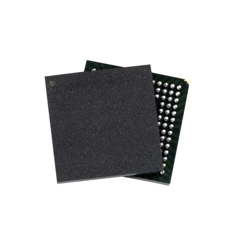
WINBOND W631GG6KB15K
DRAM Chip DDR3 SDRAM 1Gbit 64Mx16 1.5V96-Pin WBGA


Brands: WINBOND
Mfr.Part #: W631GG6KB15K
Datasheet: W631GG6KB15K Datasheet (PDF)
Package/Case: BGA
Product Type: DRAM Chip
RoHS Status:
Stock Condition: 6554 pcs, New Original
Warranty: 1 Year Ovaga Warranty - Find Out More
0
1
Add To BomW631GG6KB15K General Description
GENERAL DESCRIPTIONThe W631GG6KB is a 1G bits DDR3 SDRAM, organized as 8,388,608 words x 8 banks x 16 bits. This device achieves high speed transfer rates up to 1866 Mb/sec/pin (DDR3-1866) for various applications. W631GG6KB is sorted into the following speed grades: -11, -12, 12I, 12A, 12K -15, 15I, 15A and 15K. The -11 speed grade is compliant to the DDR3-1866 (13-13-13) specification. The -12, 12I, 12A and 12K speed grades are compliant to the DDR3-1600 (11-11-11) specification (the 12I industrial grade which is guaranteed to support -40°C ≤ TCASE ≤ 95°C). The -15, 15I, 15A and 15K speed grades are compliant to the DDR3-1333 (9-9-9) specification (the 15I industrial grade which is guaranteed to support -40°C ≤ TCASE ≤ 95°C).FEATURES Power Supply: VDD, VDDQ = 1.5V ± 0.075V Double Data Rate architecture: two data transfers per clock cycle Eight internal banks for concurrent operation 8 bit prefetch architecture CAS Latency: 6, 7, 8, 9, 10, 11 and 13 Burst length 8 (BL8) and burst chop 4 (BC4) modes: fixed via mode register (MRS) or selectable On The-Fly (OTF) Programmable read burst ordering: interleaved or nibble sequential Bi-directional, differential data strobes (DQS and DQS#) are transmitted / received with data Edge-aligned with read data and center-aligned with write data DLL aligns DQ and DQS transitions with clock Differential clock inputs (CK and CK#) Commands entered on each positive CK edge, data and data mask are referenced to both edges of a differential data strobe pair (double data rate) Posted CAS with programmable additive latency (AL = 0, CL - 1 and CL - 2) for improved command, address and data bus efficiency Read Latency = Additive Latency plus CAS Latency (RL = AL + CL) Auto-precharge operation for read and write bursts Refresh, Self-Refresh, Auto Self-refresh (ASR) and Partial array self refresh (PASR) Precharged Power Down and Active Power Down
Features
- Power Supply: VDD, VDDQ = 1.5V ± 0.075V
- Double Data Rate architecture: two data transfers per clock cycle
- Eight internal banks for concurrent operation
- 8 bit prefetch architecture
- CAS Latency: 6, 7, 8, 9, 10, 11 and 13
- Burst length 8 (BL8) and burst chop 4 (BC4) modes: fixed via mode register (MRS) or selectable On The-Fly (OTF)
- Programmable read burst ordering: interleaved or nibble sequential
- Bi-directional, differential data strobes (DQS and DQS#) are transmitted / received with data
- Edge-aligned with read data and center-aligned with write data
- DLL aligns DQ and DQS transitions with clock
- Differential clock inputs (CK and CK#)
- Commands entered on each positive CK edge, data and data mask are referenced to both edges of a differential data strobe pair (double data rate)
- Posted CAS with programmable additive latency (AL = 0, CL - 1 and CL - 2) for improved command, address and data bus efficiency
- Read Latency = Additive Latency plus CAS Latency (RL = AL + CL)
- Auto-precharge operation for read and write bursts
- Refresh, Self-Refresh, Auto Self-refresh (ASR) and Partial array self refresh (PASR)
- Precharged Power Down and Active Power Down
Specifications
| Parameter | Value | Parameter | Value |
|---|---|---|---|
| EU RoHS | Yes | RoHS Version | 2011/65/EU, 2015/863 |
| ECCN | EAR99 | Automotive | Yes |
| Supplier Cage Code | SDM39 | HTSUSA | 8542320032 |
| Schedule B | 8542320015 |
Shipping
| Shipping Type | Ship Fee | Lead Time | |
|---|---|---|---|
 |
DHL | $20.00-$40.00 (0.50 KG) | 2-5 days |
 |
Fedex | $20.00-$40.00 (0.50 KG) | 2-5 days |
 |
UPS | $20.00-$40.00 (0.50 KG) | 2-5 days |
 |
TNT | $20.00-$40.00 (0.50 KG) | 2-5 days |
 |
EMS | $20.00-$40.00 (0.50 KG) | 2-5 days |
 |
REGISTERED AIR MAIL | $20.00-$40.00 (0.50 KG) | 2-5 days |
Processing Time:Shipping fee depend on different zone and country.
Payment
| Terms of payment | Hand Fee | |
|---|---|---|
 |
Wire Transfer | charge US$30.00 banking fee. |
 |
Paypal | charge 4.0% service fee. |
 |
Credit Card | charge 3.5% service fee. |
 |
Western Union | charge US.00 banking fee. |
 |
Money Gram | charge US$0.00 banking fee. |
Guarantees
1.The electronic components you purchase include 365 Days Warranty, We guarantee product quality.
2.If some of the items you received aren't of perfect quality, we would resiponsibly arrange your refund or replacement. But the items must remain their orginal condition.
Packing
-

Step1 :Product
-

Step2 :Vacuum packaging
-

Step3 :Anti-static bag
-

Step4 :Individual packaging
-

Step5 :Packaging boxes
-

Step6 :bar-code shipping tag


All the products will packing in anti-staticbag. Ship with ESD antistatic protection.
Outside ESD packing’s lable will use ourcompany’s information: Part Mumber, Brand and Quantity.
We will inspect all the goods before shipment,ensure all the products at good condition and ensure the parts are new originalmatch datasheet.
After all the goods are ensure no problems afterpacking, we will packing safely and send by global express. It exhibitsexcellent puncture and tear resistance along with good seal integrity.


We provide high quality products, thoughtful service and after sale guarantee
-

We have rich products, can meet your various needs.
-

Minimum order quantity starts from 1pcs.
-

Lowest international shipping fee starts from $0.00
-

365 days quality guarantee for all products