Images are for reference only See Product Specifications
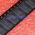
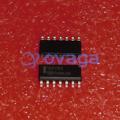
TLE2144IDW
The TLE2144IDW offers exceptional performance in terms of signal fidelity, speed, and noise reduction, making it ideal for demanding circuit designs


Brands: Texas Instruments
Mfr.Part #: TLE2144IDW
Datasheet: TLE2144IDW Datasheet (PDF)
Package/Case: SOIC (DW)-16
RoHS Status:
Stock Condition: 6227 pcs, New Original
Warranty: 1 Year Ovaga Warranty - Find Out More
0
1
Add To BomTLE2144IDW General Description
The TLE214x and TLE214xA devices are high-performance, internally compensated operational amplifiers built using Texas Instruments complementary bipolar Excalibur process. The TLE214xA is a tighter offset voltage grade of the TLE214x. Both are pin-compatible upgrades to standard industry products.
The design incorporates an input stage that simultaneously achieves low audio-band noise of 10.5 nV//100-pF load is useful in fast actuator/positioning drivers. Under similar test conditions, settling time to 0.01% is 400 ns.
The devices are stable with capacitive loads up to 10 nF, although the 6-MHz bandwidth decreases to 1.8 MHz at this high loading level. As such, the TLE214x and TLE214xA are useful for low-droop sample-and-holds and direct buffering of long cables, including 4-mA to 20-mA current loops.
The special design also exhibits an improved insensitivity to inherent integrated circuit component mismatches as is evidenced by a 500-µV maximum offset voltage and 1.7-µV/°C typical drift. Minimum common-mode rejection ratio and supply-voltage rejection ratio are 85 dB and 90 dB, respectively.
Device performance is relatively independent of supply voltage over the ±2-V to ±22-V range. Inputs can operate between VCC 0.3 to VCC+ 1.8 V without inducing phase reversal, although excessive input current may flow out of each input exceeding the lower common-mode input range. The all-npn output stage provides a nearly rail-to-rail output swing of VCC 0.1 to VCC+ 1 V under light current-loading conditions. The device can sustain shorts to either supply since output current is internally limited, but care must be taken to ensure that maximum package power dissipation is not exceeded.
Both versions can also be used as comparators. Differential inputs of VCC± can be maintained without damage to the device. Open-loop propagation delay with TTL supply levels is typically 200 ns. This gives a good indication as to output stage saturation recovery when the device is driven beyond the limits of recommended output swing.
Both the TLE214x and TLE214xA are available in a wide variety of packages, including both the industry-standard 8-pin small-outline version and chip form for high-density system applications. The C-suffix devices are characterized for operation from 0°C to 70°C, I-suffix devices from 40°C to 105°C, and M-suffix devices over the full military temperature range of 55°C to 125°C.
Features
- Low Noise
- 10 Hz.15 nV/Hz\
- 1 kHz.10.5 nV/Hz\
- 10000-pF Load Capability
- 20-mA Min Short-Circuit Output Current
- 27-V/µs Min Slew Rate
- High Gain-Bandwidth Product.5.9 MHz
- Low VIO .500 µV Max at 25°C
- Single or Split Supply.4 V to 44 V
- Fast Settling Time
- 340 ns to 0.1%
- 400 ns to 0.01%
- Saturation Recovery.150 ns
- Large Output Swing
- VCC– +0.1 V to VCC+ –1 V
Application
Specifications
| Parameter | Value | Parameter | Value |
|---|---|---|---|
| Number of channels | 4 | Total supply voltage (+5 V = 5, ±5 V = 10) (max) (V) | 44 |
| Total supply voltage (+5 V = 5, ±5 V = 10) (min) (V) | 4 | Rail-to-rail | In to V- |
| GBW (typ) (MHz) | 6 | Slew rate (typ) (V/µs) | 45 |
| Vos (offset voltage at 25°C) (max) (mV) | 2.4 | Iq per channel (typ) (mA) | 3.45 |
| Vn at 1 kHz (typ) (nV√Hz) | 10.5 | Rating | Catalog |
| Operating temperature range (°C) | -40 to 105, 0 to 70 | Offset drift (typ) (µV/°C) | 1.7 |
| Features | High Cload Drive | Input bias current (max) (pA) | 1500000 |
| CMRR (typ) (dB) | 108 | Iout (typ) (A) | 0.031 |
| Architecture | Bipolar | Input common mode headroom (to negative supply) (typ) (V) | -0.3 |
| Input common mode headroom (to positive supply) (typ) (V) | -1.8 | Output swing headroom (to negative supply) (typ) (V) | 0.1 |
| Output swing headroom (to positive supply) (typ) (V) | -0.8 |
Shipping
| Shipping Type | Ship Fee | Lead Time | |
|---|---|---|---|
 |
DHL | $20.00-$40.00 (0.50 KG) | 2-5 days |
 |
Fedex | $20.00-$40.00 (0.50 KG) | 2-5 days |
 |
UPS | $20.00-$40.00 (0.50 KG) | 2-5 days |
 |
TNT | $20.00-$40.00 (0.50 KG) | 2-5 days |
 |
EMS | $20.00-$40.00 (0.50 KG) | 2-5 days |
 |
REGISTERED AIR MAIL | $20.00-$40.00 (0.50 KG) | 2-5 days |
Processing Time:Shipping fee depend on different zone and country.
Payment
| Terms of payment | Hand Fee | |
|---|---|---|
 |
Wire Transfer | charge US$30.00 banking fee. |
 |
Paypal | charge 4.0% service fee. |
 |
Credit Card | charge 3.5% service fee. |
 |
Western Union | charge US.00 banking fee. |
 |
Money Gram | charge US$0.00 banking fee. |
Guarantees
1.The electronic components you purchase include 365 Days Warranty, We guarantee product quality.
2.If some of the items you received aren't of perfect quality, we would resiponsibly arrange your refund or replacement. But the items must remain their orginal condition.
Packing
-

Step1 :Product
-

Step2 :Vacuum packaging
-

Step3 :Anti-static bag
-

Step4 :Individual packaging
-

Step5 :Packaging boxes
-

Step6 :bar-code shipping tag


All the products will packing in anti-staticbag. Ship with ESD antistatic protection.
Outside ESD packing’s lable will use ourcompany’s information: Part Mumber, Brand and Quantity.
We will inspect all the goods before shipment,ensure all the products at good condition and ensure the parts are new originalmatch datasheet.
After all the goods are ensure no problems afterpacking, we will packing safely and send by global express. It exhibitsexcellent puncture and tear resistance along with good seal integrity.


We provide high quality products, thoughtful service and after sale guarantee
-

We have rich products, can meet your various needs.
-

Minimum order quantity starts from 1pcs.
-

Lowest international shipping fee starts from $0.00
-

365 days quality guarantee for all products