Images are for reference only See Product Specifications
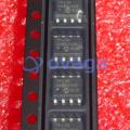
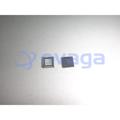
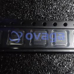
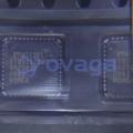
Microchip SY89833LMG
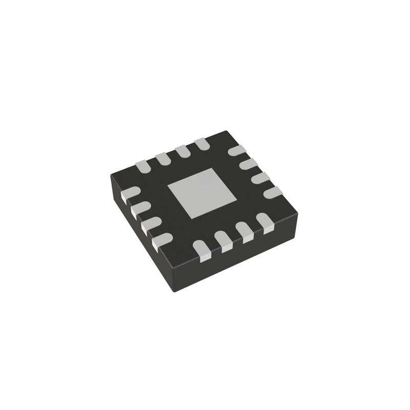
Clock Fanout Buffer 4-OUT 1-IN 1:4 16-Pin QFN EP Tube


Brands: Microchip Technology, Inc
Mfr.Part #: SY89833LMG
Datasheet: SY89833LMG Datasheet (PDF)
Package/Case: VQFN-16
Product Type: Clock & Timer ICs
RoHS Status:
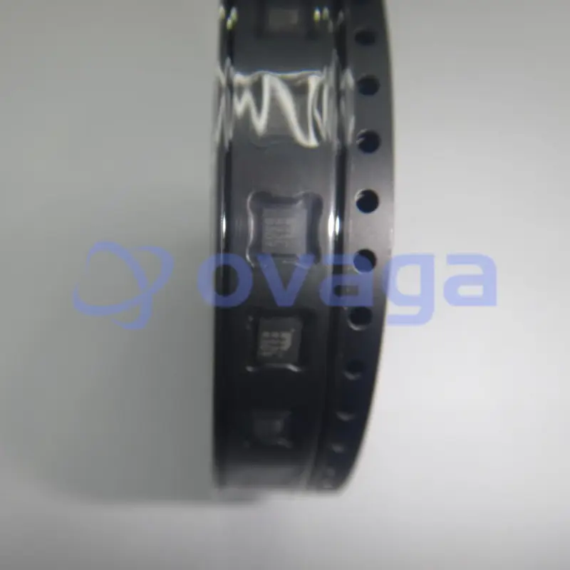
Stock Condition: 3797 pcs, New Original
Warranty: 1 Year Ovaga Warranty - Find Out More
0
1
Add To BomSY89833LMG General Description
The SY89833L is a 3.3V, high-speed 2GHz differential Low Voltage Differential Swing (LVDS) 1:4 fanout buffer optimized for ultra-low skew applications. Within device skew is guaranteed to be less than 20ps over supply voltage and temperature.The differential input buffer has a unique internal termination design that allows access to the termination network through a VT pin. This feature allows the device to easily interface to different logic standards. A VREF-AC reference is included for AC-coupled applications.The SY89833L is part of Micrel's high-speed clock synchronization family. For 2.5V applications, the SY89832U provides similar functionality while operating from a 2.5V ±5% supply. For applications that require a different I/O combination, choose from a comprehensive product line of highspeed, low-skew fanout buffers, translators and clock generators.
Features
- DC-to >2GHz throughput
- <600ps propagation delay (IN-to-Q)
- <20ps within-device skew
- <190ps rise/fall times
- 98fsRMS phase jitter
- Unique input termination and VTpin accepts DC and AC-coupled inputs
- High-speed LVDS outputs
- 3.3V power supply operation
- Industrial temperature range: -40°C to +85°C
- Available in 16-pin (3mm x 3mm) QFN package

Specifications
| Parameter | Value | Parameter | Value |
|---|---|---|---|
| Source Content uid | SY89833LMG | Rohs Code | Yes |
| Part Life Cycle Code | Active | Ihs Manufacturer | MICROCHIP TECHNOLOGY INC |
| Reach Compliance Code | compliant | ECCN Code | EAR99 |
| HTS Code | 8542.39.00.01 | Factory Lead Time | 24 Weeks |
| Samacsys Manufacturer | Microchip | Family | 89833 |
| Input Conditioning | DIFFERENTIAL | JESD-30 Code | S-XQCC-N16 |
| JESD-609 Code | e4 | Length | 3 mm |
| Logic IC Type | LOW SKEW CLOCK DRIVER | Moisture Sensitivity Level | 2 |
| Number of Functions | 1 | Number of Inverted Outputs | |
| Number of Terminals | 16 | Number of True Outputs | 4 |
| Operating Temperature-Max | 85 °C | Operating Temperature-Min | -40 °C |
| Package Body Material | UNSPECIFIED | Package Code | HVQCCN |
| Package Shape | SQUARE | Package Style | CHIP CARRIER, HEAT SINK/SLUG, VERY THIN PROFILE |
| Packing Method | TUBE | Peak Reflow Temperature (Cel) | 260 |
| Propagation Delay (tpd) | 0.6 ns | Qualification Status | Not Qualified |
| Same Edge Skew-Max (tskwd) | 0.02 ns | Seated Height-Max | 0.95 mm |
| Supply Voltage-Max (Vsup) | 3.6 V | Supply Voltage-Min (Vsup) | 3 V |
| Supply Voltage-Nom (Vsup) | 3.3 V | Surface Mount | YES |
| Temperature Grade | INDUSTRIAL | Terminal Finish | NICKEL PALLADIUM GOLD |
| Terminal Form | NO LEAD | Terminal Pitch | 0.5 mm |
| Terminal Position | QUAD | Time@Peak Reflow Temperature-Max (s) | 40 |
| Width | 3 mm | fmax-Min | 2000 MHz |
| Manufacturer: | Microchip | Product Category: | Clock Buffer |
| RoHS: | Details | Series: | SY89833 |
| Number of Outputs: | 4 Output | Maximum Input Frequency: | 2 GHz |
| Supply Voltage - Max: | 3.6 V | Supply Voltage - Min: | 3 V |
| Propagation Delay - Max: | 600 ps | Minimum Operating Temperature: | - 40 C |
| Maximum Operating Temperature: | + 85 C | Mounting Style: | SMD/SMT |
| Package / Case: | MLF-16 | Brand: | Microchip Technology |
| Moisture Sensitive: | Yes | Operating Supply Current: | 75 mA |
| Packaging: | Tube | Product: | Fanout Buffers |
| Product Type: | Clock Buffers | Factory Pack Quantity: | 100 |
| Subcategory: | Clock & Timer ICs |
Shipping
| Shipping Type | Ship Fee | Lead Time | |
|---|---|---|---|
 |
DHL | $20.00-$40.00 (0.50 KG) | 2-5 days |
 |
Fedex | $20.00-$40.00 (0.50 KG) | 2-5 days |
 |
UPS | $20.00-$40.00 (0.50 KG) | 2-5 days |
 |
TNT | $20.00-$40.00 (0.50 KG) | 2-5 days |
 |
EMS | $20.00-$40.00 (0.50 KG) | 2-5 days |
 |
REGISTERED AIR MAIL | $20.00-$40.00 (0.50 KG) | 2-5 days |
Processing Time:Shipping fee depend on different zone and country.
Payment
| Terms of payment | Hand Fee | |
|---|---|---|
 |
Wire Transfer | charge US$30.00 banking fee. |
 |
Paypal | charge 4.0% service fee. |
 |
Credit Card | charge 3.5% service fee. |
 |
Western Union | charge US.00 banking fee. |
 |
Money Gram | charge US$0.00 banking fee. |
Guarantees
1.The electronic components you purchase include 365 Days Warranty, We guarantee product quality.
2.If some of the items you received aren't of perfect quality, we would resiponsibly arrange your refund or replacement. But the items must remain their orginal condition.
Packing
-

Step1 :Product
-

Step2 :Vacuum packaging
-

Step3 :Anti-static bag
-

Step4 :Individual packaging
-

Step5 :Packaging boxes
-

Step6 :bar-code shipping tag


All the products will packing in anti-staticbag. Ship with ESD antistatic protection.
Outside ESD packing’s lable will use ourcompany’s information: Part Mumber, Brand and Quantity.
We will inspect all the goods before shipment,ensure all the products at good condition and ensure the parts are new originalmatch datasheet.
After all the goods are ensure no problems afterpacking, we will packing safely and send by global express. It exhibitsexcellent puncture and tear resistance along with good seal integrity.


Part points
-
The SY89833LMG is a high-speed, low-power 2.488Gbps LVPECL to LVDS converter chip commonly used in telecommunications and networking applications. It features a wide input common-mode range, low jitter, and high sensitivity, making it ideal for converting signals between different communication standards. The chip is available in a small form factor package for easy integration into electronic systems.
-
Equivalent
Some equivalent products of the SY89833LMG chip are the SN65LVDS32, SN65LVDS33, and SN65LVDS3487. These chips are LVDS receivers that are compatible with the SY89833LMG in various applications such as video transmission and high-speed data communication. -
Features
1. Low voltage differential PECL/LVPECL input 2. Wide input data alignment range 3. Low jitter generation and propagation 4. Power supply options: 2.5V or 3.3V 5. Clock frequency support up to 2.5GHz -
Pinout
The SY89833LMG is a 32-pin quad flat no-lead (QFN) package. It is a multi-rate channelized STM-16/OC-48 phase-locked loop (PLL) with integrated VCXO and limiting amplifiers designed for SONET/SDH networks. The device enables jitter attenuation and clock and data recovery for high-speed networking applications. -
Manufacturer
Microchip Technology is the manufacturer of the SY89833LMG. It is a semiconductor company that produces a wide range of products including microcontrollers, analog and digital ICs, and memory storage solutions for various applications in automotive, industrial, consumer, and communications sectors. -
Application Field
The SY89833LMG is commonly used in clock and data distribution systems, high-speed data transmission applications, and networking equipment such as routers, switches, and transceivers. It is also suitable for use in telecommunications, industrial automation, and test and measurement equipment due to its high-speed performance and low jitter characteristics. -
Package
The SY89833LMG chip is available in a 32-WFQFN package with a die form. The size of the chip is 5mm x 5mm.
We provide high quality products, thoughtful service and after sale guarantee
-

We have rich products, can meet your various needs.
-

Minimum order quantity starts from 1pcs.
-

Lowest international shipping fee starts from $0.00
-

365 days quality guarantee for all products