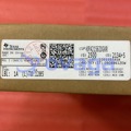
Orders Over
$5000TI OPA2325IDR
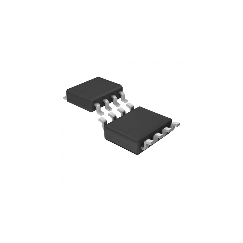
Dual precision, wide bandwidth, low noise, low power ADC driving op amp with RRIO and zero-crossover


RoHS Status:
Stock Condition: 9,768 pcs, New Original
Warranty: 1 Year Ovaga Warranty - Find Out More
0
1
OPA2325IDR General Description
The OPA325, OPA2325, and OPA4325 (OPAx325) are precision, low-voltage complementary metal-oxide semiconductor (CMOS) operational amplifiers optimized for very low noise and wide bandwidth, while operating on a low quiescent current of only 650 µA.
The OPAx325 feature a linear input stage with zero-crossover distortion that delivers excellent common-mode rejection ratio (CMRR) of typically 114 dB over the entire input range. The input common-mode range extends 100 mV beyond the negative and positive supply rails. The output voltage typically swings within 10 mV of the rails.
The zero-crossover distortion, combined with wide bandwidth (10 MHz), high slew rate (5 V/µs), and low noise (9 nV/√Hz), make the OPAx325 a very good successive-approximation register (SAR) analog-to-digital converter (ADC) input driver amplifier. In addition, the OPAx325 have a wide supply-voltage range from 2.2 V to 5.5 V, with excellent power-supply rejection ratio (PSRR) over the entire supply range, making the device an excellent choice for precision, low-power applications that run directly from batteries without regulation.
The OPA325 (single-channel version) is available in the SOT23-5 package. The OPA2325 (dual-channel version) is offered in SO-8 and MSOP-8 packages. The OPA4325 (quad-channel version) is available in TSSOP-14 package.
Features
- Precision with zero-crossover distortion:
- Low offset voltage: 150 µV (maximum)
- High CMRR: 114 dB
- Rail-to-rail I/O
- Wide bandwidth: 10 MHz
- Quiescent current: 650 µA/ch
- Single-supply voltage range: 2.2 V to 5.5 V
- Low input bias current: 0.2 pA
- Low noise: 9 nV/√Hz at 10 kHz
- Slew rate: 5 V/µs
- Unity-gain stable
Specifications
| Parameter | Value | Parameter | Value |
|---|---|---|---|
| Number of channels | 2 | Total supply voltage (+5 V = 5, ±5 V = 10) (max) (V) | 5.5 |
| Total supply voltage (+5 V = 5, ±5 V = 10) (min) (V) | 2.2 | Vos (offset voltage at 25°C) (max) (mV) | 0.15 |
| GBW (typ) (MHz) | 10 | Features | Zero Crossover |
| Slew rate (typ) (V/µs) | 5 | Rail-to-rail | In, Out |
| Offset drift (typ) (µV/°C) | 2 | Iq per channel (typ) (mA) | 0.65 |
| Vn at 1 kHz (typ) (nV√Hz) | 10 | CMRR (typ) (dB) | 114 |
| Rating | Catalog | Operating temperature range (°C) | -40 to 125 |
| Input bias current (max) (pA) | 10 | Iout (typ) (A) | 0.03 |
| Architecture | CMOS | Input common mode headroom (to negative supply) (typ) (V) | -0.1 |
| Input common mode headroom (to positive supply) (typ) (V) | 0.1 | Output swing headroom (to negative supply) (typ) (V) | 0.01 |
| Output swing headroom (to positive supply) (typ) (V) | -0.01 |
Shipping
| Shipping Type | Ship Fee | Lead Time | |
|---|---|---|---|
 |
DHL | $20.00-$40.00 (0.50 KG) | 2-5 days |
 |
Fedex | $20.00-$40.00 (0.50 KG) | 2-5 days |
 |
UPS | $20.00-$40.00 (0.50 KG) | 2-5 days |
 |
TNT | $20.00-$40.00 (0.50 KG) | 2-5 days |
 |
EMS | $20.00-$40.00 (0.50 KG) | 2-5 days |
 |
REGISTERED AIR MAIL | $20.00-$40.00 (0.50 KG) | 2-5 days |
Processing Time:Shipping fee depend on different zone and country.
Payment
| Terms of payment | Hand Fee | |
|---|---|---|
 |
Wire Transfer | charge US$30.00 banking fee. |
 |
Paypal | charge 4.0% service fee. |
 |
Credit Card | charge 3.5% service fee. |
 |
Western Union | charge US.00 banking fee. |
 |
Money Gram | charge US$0.00 banking fee. |
Guarantees
1.The electronic components you purchase include 365 Days Warranty, We guarantee product quality.
2.If some of the items you received aren't of perfect quality, we would resiponsibly arrange your refund or replacement. But the items must remain their orginal condition.
Packing
-
![Product Product]()
Step1 :Product
-
![Vacuum packaging Vacuum packaging]()
Step2 :Vacuum packaging
-
![Anti-static bag Anti-static bag]()
Step3 :Anti-static bag
-
![Individual packaging Individual packaging]()
Step4 :Individual packaging
-
![Packaging boxes Packaging boxes]()
Step5 :Packaging boxes
-
![bar-code shipping tag bar-code shipping tag]()
Step6 :bar-code shipping tag
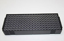
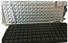
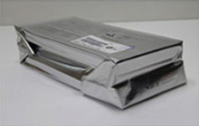
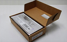
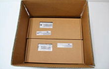
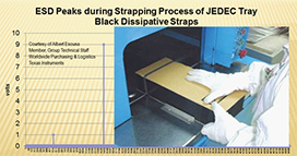
All the products will packing in anti-staticbag. Ship with ESD antistatic protection.
Outside ESD packing’s lable will use ourcompany’s information: Part Mumber, Brand and Quantity.
We will inspect all the goods before shipment,ensure all the products at good condition and ensure the parts are new originalmatch datasheet.
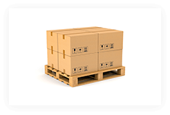
After all the goods are ensure no problems afterpacking, we will packing safely and send by global express. It exhibitsexcellent puncture and tear resistance along with good seal integrity.
We provide high quality products, thoughtful service and after sale guarantee
-
![Product Product]()
We have rich products, can meet your various needs.
-
![quantity quantity]()
Minimum order quantity starts from 1pcs.
-
![shipping shipping]()
Lowest international shipping fee starts from $0.00
-
![guarantee guarantee]()
365 days quality guarantee for all products


