Images are for reference only See Product Specifications
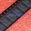
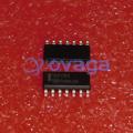
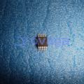
ON NB100LVEP91MNG
Translation - Voltage Levels 2.5V/3.3V Any LVL to -2.5V/-3.3V/-5V NEC


Brands: ON Semiconductor, LLC
Mfr.Part #: NB100LVEP91MNG
Datasheet: NB100LVEP91MNG Datasheet (PDF)
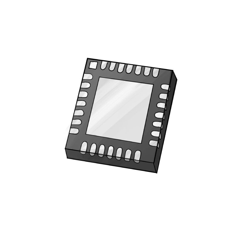
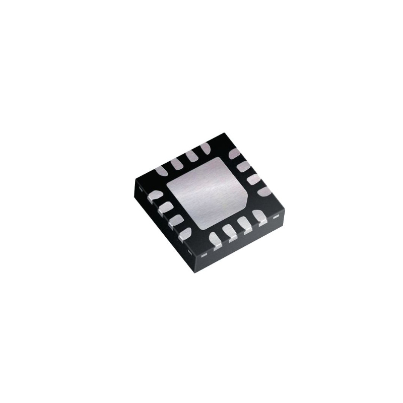
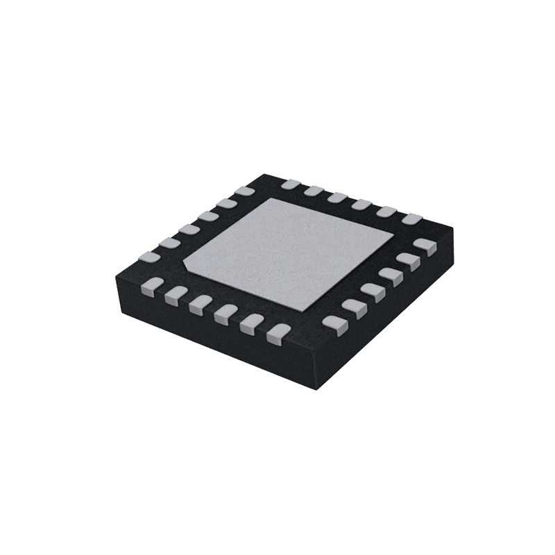
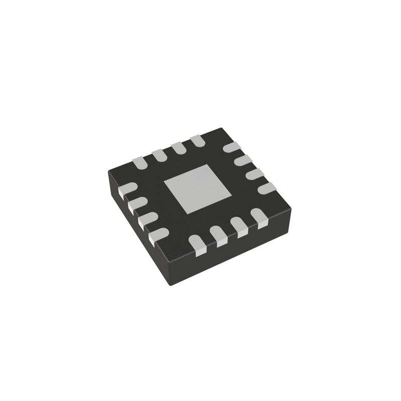
Package/Case: QFN EP
Product Type: Logic ICs
RoHS Status:
Stock Condition: 2742 pcs, New Original
Warranty: 1 Year Ovaga Warranty - Find Out More
0
1
Add To BomNB100LVEP91MNG General Description
The NB100LVEP91 is a triple input to NECL output translator. The device accepts LVPECL, LVTTL, HSTL, CML or LVDS signals, and translates them to differential -2.5 V / -3.3 V NECL output signals.
To accomplish the level translation, the LVEP91 requires three power rails. The VCC supply should be connected to the positive supply, and the VEE pin should be connected to the negative power supply. The GNDI pins are connected to the system ground plane. Both VEE and VCC should be bypassed to ground via 0.01 uF capacitors.
Under open input conditions, the Dbar input will be biased at VCC/2 and the D input will be pulled to GND. This condition will force the Q output to a low, ensuring stability.
The VBB pin, an internally generated voltage supply, is available to this device only. For single-ended input conditions, the unused differential input is connected to VBB as a switching reference voltage. VBB may also rebias AC coupled inputs. When used, decouple VBB and VCC via a 0.01 uF capacitor and limit current sourcing or sinking to 0.5 mA. When not used, VBB should be left open.
Features
- Typical Maximum Frequency >2 GHz
- 430 ps Typical Propagation Delay
- Operating Range: VCC = 2.375 V to 3.8 V; VEE = -2.375 V to -3.8 V; GNDI = 0 V
- Q Output will default LOW with Inputs Open or at GND
- Pb-Free Packages are Available
Application
ONSEMISpecifications
| Parameter | Value | Parameter | Value |
|---|---|---|---|
| Status | Active | CAD Models | |
| Compliance | PbAHP | Package Type | QFN-24 |
| Case Outline | 485L-01 | MSL Type | 1 |
| MSL Temp (°C) | 260 | Container Type | TUBE |
| Container Qty. | 92 | ON Target | Y |
| Channels | 3 | Input Level | LVDS |
| Output Level | ECL | VCC Typ (V) | 3.3 |
| fMax Typ (MHz) | 2500 | tpd Typ (ns) | 0.5 |
| tR & tF Max (ps) | 250 |
Shipping
| Shipping Type | Ship Fee | Lead Time | |
|---|---|---|---|
 |
DHL | $20.00-$40.00 (0.50 KG) | 2-5 days |
 |
Fedex | $20.00-$40.00 (0.50 KG) | 2-5 days |
 |
UPS | $20.00-$40.00 (0.50 KG) | 2-5 days |
 |
TNT | $20.00-$40.00 (0.50 KG) | 2-5 days |
 |
EMS | $20.00-$40.00 (0.50 KG) | 2-5 days |
 |
REGISTERED AIR MAIL | $20.00-$40.00 (0.50 KG) | 2-5 days |
Processing Time:Shipping fee depend on different zone and country.
Payment
| Terms of payment | Hand Fee | |
|---|---|---|
 |
Wire Transfer | charge US$30.00 banking fee. |
 |
Paypal | charge 4.0% service fee. |
 |
Credit Card | charge 3.5% service fee. |
 |
Western Union | charge US.00 banking fee. |
 |
Money Gram | charge US$0.00 banking fee. |
Guarantees
1.The electronic components you purchase include 365 Days Warranty, We guarantee product quality.
2.If some of the items you received aren't of perfect quality, we would resiponsibly arrange your refund or replacement. But the items must remain their orginal condition.
Packing
-

Step1 :Product
-

Step2 :Vacuum packaging
-

Step3 :Anti-static bag
-

Step4 :Individual packaging
-

Step5 :Packaging boxes
-

Step6 :bar-code shipping tag


All the products will packing in anti-staticbag. Ship with ESD antistatic protection.
Outside ESD packing’s lable will use ourcompany’s information: Part Mumber, Brand and Quantity.
We will inspect all the goods before shipment,ensure all the products at good condition and ensure the parts are new originalmatch datasheet.
After all the goods are ensure no problems afterpacking, we will packing safely and send by global express. It exhibitsexcellent puncture and tear resistance along with good seal integrity.


We provide high quality products, thoughtful service and after sale guarantee
-

We have rich products, can meet your various needs.
-

Minimum order quantity starts from 1pcs.
-

Lowest international shipping fee starts from $0.00
-

365 days quality guarantee for all products