Images are for reference only See Product Specifications
ON MUN5315DW1T1G

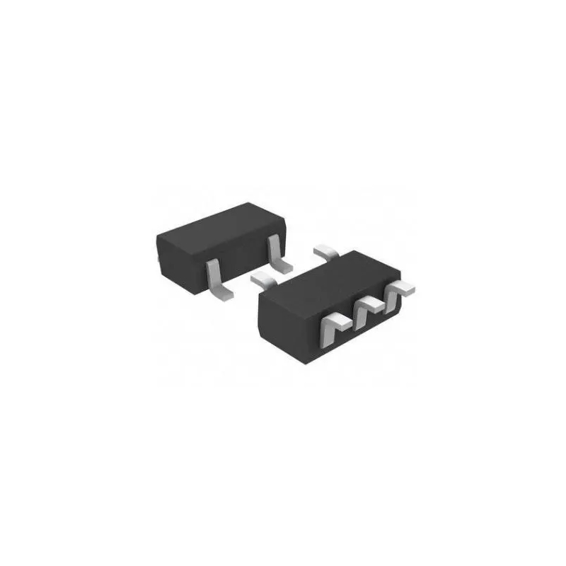
Trans Digital BJT NPN/PNP: MUN5315DW1T1G, 50V, 100mA, 6-Pin SOT-363, Tape and Reel


Brands: Onsemi
Mfr.Part #: MUN5315DW1T1G
Datasheet: MUN5315DW1T1G Datasheet (PDF)
Package/Case: SC-88-6
RoHS Status:
Stock Condition: 2526 pcs, New Original
Product Type: Transistors
Warranty: 1 Year Ovaga Warranty - Find Out More
0
1
*All prices are in USD
| Qty | Unit Price | Ext Price |
|---|---|---|
| 1 | $0.095 | $0.095 |
| 200 | $0.037 | $7.400 |
| 500 | $0.036 | $18.000 |
| 1000 | $0.035 | $35.000 |
In Stock:2526 PCS
MUN5315DW1T1G General Description
The MUN5315DW1T1G is a dual N-channel MOSFET transistor manufactured by ON Semiconductor. It is designed for general-purpose switching applications that require low on-resistance and high power handling capability. This MOSFET has a drain-to-source voltage (VDS) rating of 30 volts and a continuous drain current (ID) rating of 3.7 amperes.The MUN5315DW1T1G features a low gate threshold voltage of 1.5 volts, making it suitable for driving with low-voltage logic signals. It has a low on-resistance of 0.063 ohms to minimize power dissipation and improve efficiency in switching applications.This dual MOSFET comes in a small DFN package with dimensions of 2mm x 2mm, making it suitable for space-constrained applications. It has a maximum operating temperature of 150 degrees Celsius, ensuring reliable performance in a variety of operating conditions.
Features
Application
Specifications
| Parameter | Value | Parameter | Value |
|---|---|---|---|
| Product Category | Digital Transistors | RoHS | Details |
| Configuration | Dual | Transistor Polarity | NPN, PNP |
| Typical Input Resistor | 10 kOhms | Mounting Style | SMD/SMT |
| Package / Case | SC-88-6 | DC Collector/Base Gain hfe Min | 160 |
| Collector- Emitter Voltage VCEO Max | 50 V | Continuous Collector Current | 100 mA |
| Peak DC Collector Current | 100 mA | Pd - Power Dissipation | 187 mW |
| Minimum Operating Temperature | - 55 C | Maximum Operating Temperature | + 150 C |
| Series | MUN5315DW1 | Brand | onsemi |
| DC Current Gain hFE Max | 160 at 5 mA at 10 V | Height | 0.9 mm |
| Length | 2 mm | Number of Channels | 2 Channel |
| Product Type | Digital Transistors | Factory Pack Quantity | 3000 |
| Subcategory | Transistors | Width | 1.25 mm |
| Unit Weight | 0.000219 oz |
Shipping
| Shipping Type | Ship Fee | Lead Time | |
|---|---|---|---|
 |
DHL | $20.00-$40.00 (0.50 KG) | 2-5 days |
 |
Fedex | $20.00-$40.00 (0.50 KG) | 2-5 days |
 |
UPS | $20.00-$40.00 (0.50 KG) | 2-5 days |
 |
TNT | $20.00-$40.00 (0.50 KG) | 2-5 days |
 |
EMS | $20.00-$40.00 (0.50 KG) | 2-5 days |
 |
REGISTERED AIR MAIL | $20.00-$40.00 (0.50 KG) | 2-5 days |
Processing Time:Shipping fee depend on different zone and country.
Payment
| Terms of payment | Hand Fee | |
|---|---|---|
 |
Wire Transfer | charge US$30.00 banking fee. |
 |
Paypal | charge 4.0% service fee. |
 |
Credit Card | charge 3.5% service fee. |
 |
Western Union | charge US.00 banking fee. |
 |
Money Gram | charge US$0.00 banking fee. |
Guarantees
1.The electronic components you purchase include 365 Days Warranty, We guarantee product quality.
2.If some of the items you received aren't of perfect quality, we would resiponsibly arrange your refund or replacement. But the items must remain their orginal condition.
Packing
-

Step1 :Product
-

Step2 :Vacuum packaging
-

Step3 :Anti-static bag
-

Step4 :Individual packaging
-

Step5 :Packaging boxes
-

Step6 :bar-code shipping tag


All the products will packing in anti-staticbag. Ship with ESD antistatic protection.
Outside ESD packing’s lable will use ourcompany’s information: Part Mumber, Brand and Quantity.
We will inspect all the goods before shipment,ensure all the products at good condition and ensure the parts are new originalmatch datasheet.
After all the goods are ensure no problems afterpacking, we will packing safely and send by global express. It exhibitsexcellent puncture and tear resistance along with good seal integrity.


Part points
-
The MUN5315DW1T1G chip is an NPN lownoise amplifier transistor designed for applications in wireless communication systems. It operates in the frequency range of 900MHz to 2GHz and offers a low noise figure of 1.1dB, making it suitable for sensitive signal amplification. The chip is housed in a small SOT-323 package, which enables compact designs for space-constrained applications.
-
Features
The MUN5315DW1T1G is a NPN Bipolar Power Transistor with a high collector current capability of 5A, low saturation voltage, and fast switching speed. It is designed for general-purpose amplifier and switching applications in power supply systems, motor control, and consumer electronics. -
Pinout
The MUN5315DW1T1G is a dual NPN/PNP bipolar transistor with 6 pins. The first 3 pins are for connection to the NPN transistor, and the last 3 pins are for connection to the PNP transistor. The device is designed for switching applications in automotive and general-purpose use. -
Manufacturer
The manufacturer of the MUN5315DW1T1G is ON Semiconductor. It is a multinational semiconductor supplier company. -
Application Field
The MUN5315DW1T1G is an NPN bipolar transistor commonly used in a variety of applications, including switching and amplification circuits, power management systems, and in various electronic devices requiring high voltage and current capabilities. -
Package
The MUN5315DW1T1G chip is available in a SOT-363 package, which is a small surface-mount package. The chip has a form factor of a small rectangular shape with four terminals. The overall package size is approximately 2.0mm x 1.25mm x 0.75mm.


Datasheet PDF
We provide high quality products, thoughtful service and after sale guarantee
-

We have rich products, can meet your various needs.
-

Minimum order quantity starts from 1pcs.
-

Lowest international shipping fee starts from $0.00
-

365 days quality guarantee for all products