Images are for reference only See Product Specifications
K9F1G08U0C-PCB0
3.3 Voltage Operation


Brands: Samsung Electronics
Mfr.Part #: K9F1G08U0C-PCB0
Datasheet: K9F1G08U0C-PCB0 Datasheet (PDF)
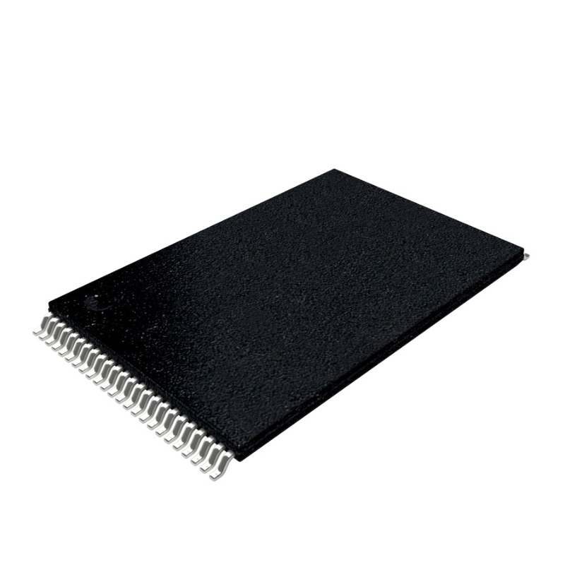
Package/Case: TSOP-I
RoHS Status:
Stock Condition: 9318 pcs, New Original
Warranty: 1 Year Ovaga Warranty - Find Out More
0
1
Add To BomK9F1G08U0C-PCB0 General Description
The K9F1G08U0C-PCB0 is a 1 Gbit NAND Flash memory chip manufactured by Samsung. It is designed for use in various electronic devices such as smartphones, tablets, digital cameras, and solid-state drives. This memory chip offers a high storage capacity of 1 Gbit or 128 MB, making it suitable for storing large amounts of data and media files.The K9F1G08U0C-PCB0 uses NAND Flash technology, which provides fast data transfer speeds and high reliability. It operates on a voltage range of 2.7V to 3.6V and features a low power consumption, making it ideal for portable devices with limited battery capacity.This memory chip has a page size of 2 KB and a block size of 64 KB, allowing for efficient data management and storage. It also supports various interface options, including Toggle and ONFI, for seamless integration with different types of devices.
Features
Application
Specifications
| Parameter | Value | Parameter | Value |
|---|---|---|---|
| ECCN (US) | 3A991.b.1.a | Part Status | Obsolete |
| Automotive | No | PPAP | No |
| Cell Type | NAND | Chip Density (bit) | 1G |
| Architecture | Sectored | Boot Block | No |
| Block Organization | Symmetrical | Address Bus Width (bit) | 28 |
| Sector Size | 128Kbyte x 1024 | Page Size | 2Kbyte |
| Number of Bits/Word (bit) | 8 | Number of Words | 128M |
| Programmability | Yes | Timing Type | Asynchronous |
| Maximum Erase Time (s) | 0.01/Block | Maximum Programming Time (ms) | 0.7 |
| Interface Type | Parallel | Minimum Operating Supply Voltage (V) | 2.7 |
| Typical Operating Supply Voltage (V) | 3.3 | Maximum Operating Supply Voltage (V) | 3.6 |
| Operating Current (mA) | 30 | Page Read Current (mA) | 30 |
| Program Current (mA) | 30 | Minimum Operating Temperature (°C) | -10 |
| Maximum Operating Temperature (°C) | 125 | Command Compatible | No |
| ECC Support | Yes | Support of Page Mode | Yes |
| Mounting | Surface Mount | Package Height | 1 |
| Package Width | 18.4 | Package Length | 12 |
| PCB changed | 48 | Standard Package Name | SO |
| Supplier Package | TSOP-I | Pin Count | 48 |
| Lead Shape | Gull-wing |
Shipping
| Shipping Type | Ship Fee | Lead Time | |
|---|---|---|---|
 |
DHL | $20.00-$40.00 (0.50 KG) | 2-5 days |
 |
Fedex | $20.00-$40.00 (0.50 KG) | 2-5 days |
 |
UPS | $20.00-$40.00 (0.50 KG) | 2-5 days |
 |
TNT | $20.00-$40.00 (0.50 KG) | 2-5 days |
 |
EMS | $20.00-$40.00 (0.50 KG) | 2-5 days |
 |
REGISTERED AIR MAIL | $20.00-$40.00 (0.50 KG) | 2-5 days |
Processing Time:Shipping fee depend on different zone and country.
Payment
| Terms of payment | Hand Fee | |
|---|---|---|
 |
Wire Transfer | charge US$30.00 banking fee. |
 |
Paypal | charge 4.0% service fee. |
 |
Credit Card | charge 3.5% service fee. |
 |
Western Union | charge US.00 banking fee. |
 |
Money Gram | charge US$0.00 banking fee. |
Guarantees
1.The electronic components you purchase include 365 Days Warranty, We guarantee product quality.
2.If some of the items you received aren't of perfect quality, we would resiponsibly arrange your refund or replacement. But the items must remain their orginal condition.
Packing
-

Step1 :Product
-

Step2 :Vacuum packaging
-

Step3 :Anti-static bag
-

Step4 :Individual packaging
-

Step5 :Packaging boxes
-

Step6 :bar-code shipping tag


All the products will packing in anti-staticbag. Ship with ESD antistatic protection.
Outside ESD packing’s lable will use ourcompany’s information: Part Mumber, Brand and Quantity.
We will inspect all the goods before shipment,ensure all the products at good condition and ensure the parts are new originalmatch datasheet.
After all the goods are ensure no problems afterpacking, we will packing safely and send by global express. It exhibitsexcellent puncture and tear resistance along with good seal integrity.


Part points
-
The K9F1G08U0C-PCB0 chip is a NAND flash memory device manufactured by Samsung. It has a capacity of 1 Gb (gigabit) and is commonly used for data storage in electronic devices such as smartphones, tablets, and other portable devices. It provides high-speed data transfer and reliable performance, making it a popular choice in the industry.
-
Equivalent
Some equivalent products of the K9F1G08U0C-PCB0 chip are K9F1G08U0D-PCB0, K9F1G08U0M-PCB0, K9F1G08U0M-YCB0, and K9F1G08U0B-JIB0. -
Features
K9F1G08U0C-PCB0 is a 1Gb NAND Flash memory device. It is designed for high-density storage applications, with a voltage range from 2.7V to 3.6V. The device offers a fast programming time, a high-speed data transfer rate, and a small page size for efficient data management. -
Pinout
The K9F1G08U0C-PCB0 is a NAND flash memory IC with a pin count of 48. It is commonly used in various electronic devices for data storage. The functions of the pins include data input/output, control signals, power supply, and ground connections. -
Manufacturer
The manufacturer of the K9F1G08U0C-PCB0 is Samsung Electronics, a multinational technology company. Samsung is primarily known for its consumer electronics products, including smartphones and televisions, but also manufactures a wide range of components and memory solutions for various industries, including the automotive, aerospace, and semiconductor sectors. -
Application Field
The K9F1G08U0C-PCB0 is commonly used in various electronic devices such as smartphones, tablets, digital cameras, and USB flash drives. It is primarily utilized as an NAND Flash memory component for data storage and retrieval purposes in these applications. -
Package
The K9F1G08U0C-PCB0 chip comes in a TSOP (Thin Small Outline Package) form, with a size of 48 pins and a body size of approximately 12mm x 20mm.
We provide high quality products, thoughtful service and after sale guarantee
-

We have rich products, can meet your various needs.
-

Minimum order quantity starts from 1pcs.
-

Lowest international shipping fee starts from $0.00
-

365 days quality guarantee for all products