


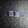
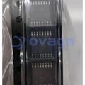
Images are for reference only See Product Specifications
Renesas HS4-3282-8
CMOS ARINC Bus Interface Circuit


Brands: Renesas Technology Corp
Mfr.Part #: HS4-3282-8
Datasheet: HS4-3282-8 Datasheet (PDF)
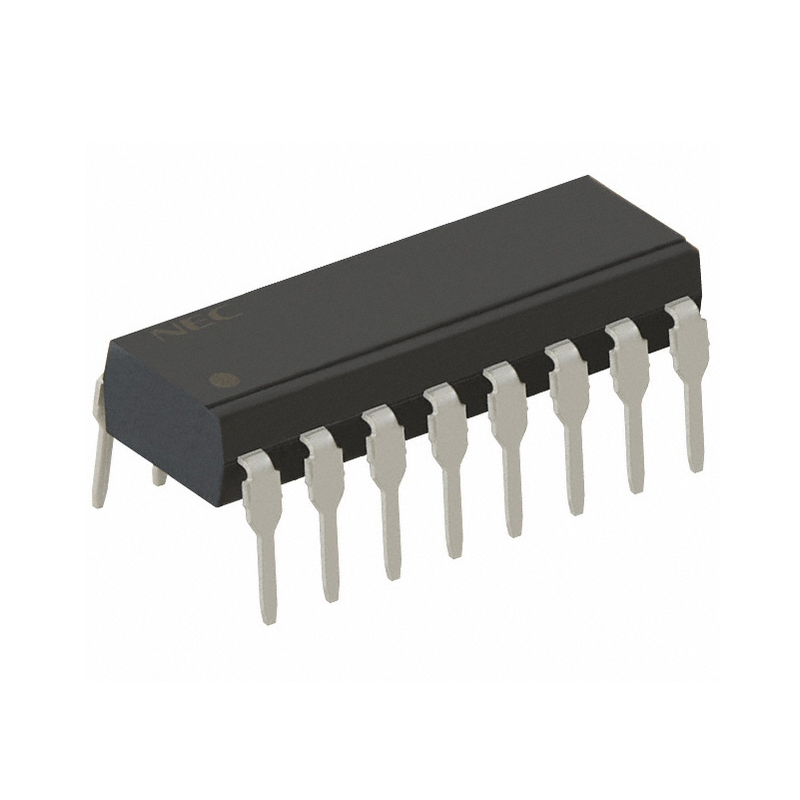
Package/Case: LCC-44
Product Type: Interface ICs
RoHS Status:
Stock Condition: 3685 pcs, New Original
Warranty: 1 Year Ovaga Warranty - Find Out More
0
1
Add To BomHS4-3282-8 General Description
The HS-3282 is a high performance CMOS bus interface circuit that is intended to meet the requirements of ARINC Specification 429, and similar encoded, time multiplexed serial data protocols. This device is intended to be used with the HS-3182, a monolithic Dl bipolar differential line driver designed to meet the specifications of ARINC 429. The ARINC 429 bus interface circuit consists of two (2) receivers and a transmitter operating independently as shown in Figure 1. The two receivers operate at a frequency that is ten (10) times the receiver data rate, which can be the same or different from the transmitter data rate. Although the two receivers operate at the same frequency, they are functionally independent and each receives serial data asynchronously. The transmitter section of the ARINC bus interface circuit consists mainly of a First-In First-Out (FIFO) memory and timing circuit. The FIFO memory is used to hold up to eight (8) ARINC data words for transmission serially. The timing circuit is used to correctly separate each ARINC word as required by ARINC Specification 429. Even though ARINC Specification 429 specifies a 32-bit word, including parity, the HS-3282 can be programmed to also operate with a word length of 25 bits. The incoming receiver data word parity is checked, and a parity status is stored in the receiver latch and output on Pin BD08 during the 1st word. [A logic 0 indicates that an odd number of logic 1 s were received and stored; a logic 1 indicates that an even number of logic 1s were received and stored]. In the transmitter the parity generator will generate either odd or even parity depending upon the status of PARCK control signal. A logic 0 on BD12 will cause odd parity to be used in the output data stream. Versatility is provided in both the transmitter and receiver by the external clock input which allows the bus interface circuit to operate at data rates from 0 to 100 kilobits. The external clock must be ten (10) times the data rate to insure no data ambiguity. The ARINC bus interface circuit is fully guaranteed to support the data rates of ARINC specification 429 over both the voltage (±5%) and full military temperature range. It interfaces with UL, CMOS or NMOS support circuitry, and uses the standard 5-volt VCC supply.
Features
- ARlNC Specification 429 Compatible
- Data Rates of 100 Kilobits or 12.5 Kilobits
- Separate Receiver and Transmitter Section
- Dual and Independent Receivers, Connecting Directly to ARINC Bus
- Serial to Parallel Receiver Data Conversion
- Parallel to Serial Transmitter Data Conversion
- Word Lengths of 25 or 32 Bits
- Parity Status of Received Data
- Generate Parity of Transmitter Data
- Automatic Word Gap Timer
- Single 5V Supply
- Low Power Dissipation
- Full Military Temperature Range
Specifications
| Parameter | Value | Parameter | Value |
|---|---|---|---|
| Manufacturer | INTERSI | Product Category | IC Chips |
| Tags | HS4-32, HS4-3, HS4 |
Shipping
| Shipping Type | Ship Fee | Lead Time | |
|---|---|---|---|
 |
DHL | $20.00-$40.00 (0.50 KG) | 2-5 days |
 |
Fedex | $20.00-$40.00 (0.50 KG) | 2-5 days |
 |
UPS | $20.00-$40.00 (0.50 KG) | 2-5 days |
 |
TNT | $20.00-$40.00 (0.50 KG) | 2-5 days |
 |
EMS | $20.00-$40.00 (0.50 KG) | 2-5 days |
 |
REGISTERED AIR MAIL | $20.00-$40.00 (0.50 KG) | 2-5 days |
Processing Time:Shipping fee depend on different zone and country.
Payment
| Terms of payment | Hand Fee | |
|---|---|---|
 |
Wire Transfer | charge US$30.00 banking fee. |
 |
Paypal | charge 4.0% service fee. |
 |
Credit Card | charge 3.5% service fee. |
 |
Western Union | charge US.00 banking fee. |
 |
Money Gram | charge US$0.00 banking fee. |
Guarantees
1.The electronic components you purchase include 365 Days Warranty, We guarantee product quality.
2.If some of the items you received aren't of perfect quality, we would resiponsibly arrange your refund or replacement. But the items must remain their orginal condition.
Packing
-

Step1 :Product
-

Step2 :Vacuum packaging
-

Step3 :Anti-static bag
-

Step4 :Individual packaging
-

Step5 :Packaging boxes
-

Step6 :bar-code shipping tag


All the products will packing in anti-staticbag. Ship with ESD antistatic protection.
Outside ESD packing’s lable will use ourcompany’s information: Part Mumber, Brand and Quantity.
We will inspect all the goods before shipment,ensure all the products at good condition and ensure the parts are new originalmatch datasheet.
After all the goods are ensure no problems afterpacking, we will packing safely and send by global express. It exhibitsexcellent puncture and tear resistance along with good seal integrity.


Part points
-
The HS4-3282-8 chip is an advanced integrated circuit designed for high-speed data communications. It features eight channels, enabling simultaneous transmission and reception of data. With its efficient design and performance capabilities, the chip is suitable for applications requiring fast and reliable data transfer, such as telecommunications, networking, and data centers.
-
Features
HS4-3282-8 is a high-speed digital multiplexer/demultiplexer that operates at a frequency of 155 MHz, with 8 input/output channels and straight-through or cross-point switching capability. It provides low crosstalk and insertion loss, supports high-speed data transmission, and is suitable for various communication systems, including SONET/SDH, ATM, and communications test equipment. -
Pinout
The HS4-3282-8 is a connector with an 8-pin count. The specific function and pinout of the connector would depend on the manufacturer and the intended application. The pin count typically refers to the number of physical pins on the connector. -
Application Field
The HS4-3282-8 can be used in various applications such as industrial automation, robotics, medical devices, and aerospace systems. Its compact size, high torque, and versatility make it suitable for demanding tasks that require precise and powerful motor control. -
Package
The HS4-3282-8 chip has a package type of QFP (Quad Flat Package), a form of square shape with a flat body, and a size of 32 x 32 mm.


Datasheet PDF
We provide high quality products, thoughtful service and after sale guarantee
-

We have rich products, can meet your various needs.
-

Minimum order quantity starts from 1pcs.
-

Lowest international shipping fee starts from $0.00
-

365 days quality guarantee for all products


Ovaga's commitment to quality and value is unmatched, fantastic supplier to work with.