Images are for reference only See Product Specifications
AOD413A
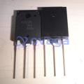
Trans MOSFET P-CH 40V 12A 3-Pin(2+Tab) DPAK


Brands: Alpha And Omega Semiconductor
Mfr.Part #: AOD413A
Datasheet: AOD413A Datasheet (PDF)
Package/Case: DPAK
RoHS Status:
Stock Condition: 5868 pcs, New Original
Warranty: 1 Year Ovaga Warranty - Find Out More
0
1
Add To BomOvaga has a large stock of AOD413A Voltage regulator tube from Alpha And Omega Semiconductor and we guarantee that they are original,brand new parts sourced directly from Alpha And Omega Semiconductor We can provide quality testing reports for AOD413A upon your request. To obtain a quote, simply fill in the required quantity, contact name, and email address in the quick quote form on the right. Our sales representative will contact you within 12 hours.
Specifications
| Parameter | Value | Parameter | Value |
|---|---|---|---|
| ECCN (US) | EAR99 | Part Status | Active |
| HTS | 8541.21.00.95 | SVHC | Yes |
| SVHC Exceeds Threshold | Yes | Automotive | No |
| PPAP | No | Category | Power MOSFET |
| Configuration | Single | Process Technology | Trench |
| Channel Mode | Enhancement | Channel Type | P |
| Number of Elements per Chip | 1 | Maximum Drain Source Voltage (V) | 40 |
| Maximum Gate Source Voltage (V) | ±20 | Maximum Gate Threshold Voltage (V) | 3 |
| Operating Junction Temperature (°C) | -55 to 175 | Maximum Continuous Drain Current (A) | 12 |
| Maximum Gate Source Leakage Current (nA) | 100 | Maximum IDSS (uA) | 1 |
| Maximum Drain Source Resistance (mOhm) | 44@10V | Typical Gate Charge @ Vgs (nC) | 16.2@10V|[email protected] |
| Typical Gate Charge @ 10V (nC) | 16.2 | Typical Gate to Drain Charge (nC) | 3.5@10V |
| Typical Gate to Source Charge (nC) | 3.8 | Typical Reverse Recovery Charge (nC) | 13.8 |
| Typical Input Capacitance @ Vds (pF) | 900@20V | Typical Reverse Transfer Capacitance @ Vds (pF) | 68@20V |
| Minimum Gate Threshold Voltage (V) | 1.7 | Typical Output Capacitance (pF) | 97 |
| Maximum Power Dissipation (mW) | 5000 | Typical Fall Time (ns) | 41.2 |
| Typical Rise Time (ns) | 8.4 | Typical Turn-Off Delay Time (ns) | 44.8 |
| Typical Turn-On Delay Time (ns) | 6.2 | Minimum Operating Temperature (°C) | -55 |
| Maximum Operating Temperature (°C) | 175 | Typical Drain Source Resistance @ 25°C (mOhm) | 36@10V|[email protected] |
| Maximum Pulsed Drain Current @ TC=25°C (A) | 30 | Maximum Junction Ambient Thermal Resistance on PCB (°C/W) | 50 |
| Typical Diode Forward Voltage (V) | 0.76 | Typical Gate Plateau Voltage (V) | 4.2 |
| Typical Reverse Recovery Time (ns) | 21.2 | Maximum Diode Forward Voltage (V) | 1 |
| Typical Gate Threshold Voltage (V) | 2 | Maximum Positive Gate Source Voltage (V) | 20 |
| Mounting | Surface Mount | Package Height | 2.29 |
| Package Width | 6.1 | Package Length | 6.6 |
| PCB changed | 2 | Tab | Tab |
| Standard Package Name | TO-252 | Supplier Package | DPAK |
| Pin Count | 3 |
Shipping
| Shipping Type | Ship Fee | Lead Time | |
|---|---|---|---|
 |
DHL | $20.00-$40.00 (0.50 KG) | 2-5 days |
 |
Fedex | $20.00-$40.00 (0.50 KG) | 2-5 days |
 |
UPS | $20.00-$40.00 (0.50 KG) | 2-5 days |
 |
TNT | $20.00-$40.00 (0.50 KG) | 2-5 days |
 |
EMS | $20.00-$40.00 (0.50 KG) | 2-5 days |
 |
REGISTERED AIR MAIL | $20.00-$40.00 (0.50 KG) | 2-5 days |
Processing Time:Shipping fee depend on different zone and country.
Payment
| Terms of payment | Hand Fee | |
|---|---|---|
 |
Wire Transfer | charge US$30.00 banking fee. |
 |
Paypal | charge 4.0% service fee. |
 |
Credit Card | charge 3.5% service fee. |
 |
Western Union | charge US.00 banking fee. |
 |
Money Gram | charge US$0.00 banking fee. |
Guarantees
1.The electronic components you purchase include 365 Days Warranty, We guarantee product quality.
2.If some of the items you received aren't of perfect quality, we would resiponsibly arrange your refund or replacement. But the items must remain their orginal condition.
Packing
-

Step1 :Product
-

Step2 :Vacuum packaging
-

Step3 :Anti-static bag
-

Step4 :Individual packaging
-

Step5 :Packaging boxes
-

Step6 :bar-code shipping tag


All the products will packing in anti-staticbag. Ship with ESD antistatic protection.
Outside ESD packing’s lable will use ourcompany’s information: Part Mumber, Brand and Quantity.
We will inspect all the goods before shipment,ensure all the products at good condition and ensure the parts are new originalmatch datasheet.
After all the goods are ensure no problems afterpacking, we will packing safely and send by global express. It exhibitsexcellent puncture and tear resistance along with good seal integrity.


We provide high quality products, thoughtful service and after sale guarantee
-

We have rich products, can meet your various needs.
-

Minimum order quantity starts from 1pcs.
-

Lowest international shipping fee starts from $0.00
-

365 days quality guarantee for all products