


Images are for reference only See Product Specifications
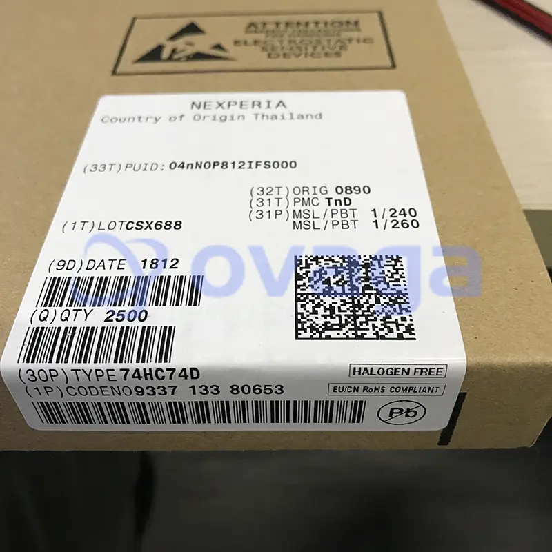
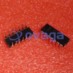
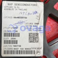
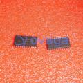
NXP 74HC74D
Flip Flop D-Type Pos-Edge 2-Element


Brands: Toshiba
Mfr.Part #: 74HC74D
Datasheet: 74HC74D Datasheet (PDF)
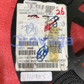
Package/Case: SOIC-14
Product Type: Logic ICs
RoHS Status:
Stock Condition: 2116 pcs, New Original
Warranty: 1 Year Ovaga Warranty - Find Out More
0
1
Add To Bom74HC74D General Description
The 74HC74 and 74HCT74 are dual positive edge-triggered D-type flip-flops, and here are some key characteristics and features:
Flip-Flop Type: They are D-type flip-flops, meaning they store and transfer data based on the clock signal. When the clock signal transitions from low to high (positive edge), the data at the D-input is captured and appears at the Q output.
Inputs and Outputs:
Data (nD): The D-type flip-flops have individual data (nD) inputs.
Clock (nCP): They have clock (nCP) inputs for triggering the flip-flops.
Set (nSD) and Reset (nRD) Inputs: These flip-flops feature set and reset inputs to set or reset the flip-flop's state.
Complementary Outputs (nQ and nQ): They provide complementary outputs, where nQ is the normal output, and nQ is the complement of nQ.
Clock Input: The clock input features Schmitt-trigger action, which makes the circuit tolerant to slower clock rise and fall times. This feature helps improve noise immunity and signal integrity.
Clamp Diodes: Inputs on these flip-flops include clamp diodes. These diodes protect the inputs and enable the use of current-limiting resistors to interface inputs with voltages that may exceed VCC. This is especially useful in applications where the input signals might vary beyond the normal operating voltage range.
Data Storage: Data at the nD-input that meets the setup and hold time requirements on the LOW-to-HIGH clock transition is stored in the flip-flop and appears at the nQ output.
These flip-flops are useful for a variety of applications in digital electronics where data needs to be stored and synchronized with a clock signal. Their compatibility with CMOS logic levels (74HC) and tolerance to slower clock edges make them versatile components for digital circuit design. Always consult the datasheet provided by the manufacturer for specific electrical characteristics and usage guidelines.
Features
Wide Supply Voltage Range: These flip-flops can operate over a wide supply voltage range from 2.0 to 6.0 V, providing flexibility in various applications.
CMOS Low Power Dissipation: They have low power dissipation characteristics, making them energy-efficient and suitable for battery-operated devices.
High Noise Immunity: These flip-flops are designed to have high noise immunity, making them less susceptible to unwanted signal fluctuations or interference.
Input Levels:
For 74HC74: The input levels are compatible with CMOS logic.
For 74HCT74: The input levels are compatible with TTL logic.
Symmetrical Output Impedance: These flip-flops have symmetrical output impedance, ensuring consistent and balanced output characteristics.
Balanced Propagation Delays: They offer balanced propagation delays, which means that the delays for signals through the flip-flop are roughly equal, contributing to signal synchronization.
Latch-Up Performance: These flip-flops have a latch-up performance that exceeds 100 mA per JESD 78 Class II Level B, ensuring robust and reliable operation.
JEDEC Standards Compliance:
JESD8C (2.7 V to 3.6 V): Compliant with these voltage standards.
JESD7A (2.0 V to 6.0 V): Compliant with these voltage standards, ensuring versatility.
ESD Protection:
HBM (Human Body Model) JESD22-A114F: Exceeds 2000 V, providing protection against electrostatic discharge.
MM (Machine Model) JESD22-A115-A: Exceeds 200 V, offering protection in various operational environments.
Multiple Package Options: These flip-flops are available in multiple package options to suit different design requirements and form factors.
Operating Temperature Range: These flip-flops are specified to operate reliably within a temperature range from -40°C to +85°C and from -40°C to +125°C, making them suitable for a wide range of environmental conditions.
Application
- Digital logic circuits: 74HC74D can be used in digital systems for tasks such as data storage, data manipulation, and data synchronization.
- Sequential logic circuits: It can be used in sequential logic circuits for tasks such as data latching, data buffering, and data synchronization.
- Clock synchronization: It can be used in clock synchronization circuits to align different clock signals in a digital system.
- Register and counter circuits: It can be used in register and counter circuits for storing and manipulating data in various applications.
Specifications
| Parameter | Value | Parameter | Value |
|---|---|---|---|
| Product Name | 74HC74D | Product Type | Dual D-Type Flip-Flop IC |
| Manufacturer | Various (e.g., Texas Instruments, NXP Semiconductors) | Number of Flip-Flops | 2 D-Type Flip-Flops (in a single IC) |
| Supply Voltage Range | 2V to 6V | Operating Temperature Range | -40°C to +125°C |
| Package / Case | SOIC-14 (Small Outline Integrated Circuit, 14-pins) | Packaging | Tube, Tape & Reel, and other options |
| Pin Count | 14 | Package Category | Small Outline Packages |
| Released Date | Feb 15, 2023 |
Shipping
| Shipping Type | Ship Fee | Lead Time | |
|---|---|---|---|
 |
DHL | $20.00-$40.00 (0.50 KG) | 2-5 days |
 |
Fedex | $20.00-$40.00 (0.50 KG) | 2-5 days |
 |
UPS | $20.00-$40.00 (0.50 KG) | 2-5 days |
 |
TNT | $20.00-$40.00 (0.50 KG) | 2-5 days |
 |
EMS | $20.00-$40.00 (0.50 KG) | 2-5 days |
 |
REGISTERED AIR MAIL | $20.00-$40.00 (0.50 KG) | 2-5 days |
Processing Time:Shipping fee depend on different zone and country.
Payment
| Terms of payment | Hand Fee | |
|---|---|---|
 |
Wire Transfer | charge US$30.00 banking fee. |
 |
Paypal | charge 4.0% service fee. |
 |
Credit Card | charge 3.5% service fee. |
 |
Western Union | charge US.00 banking fee. |
 |
Money Gram | charge US$0.00 banking fee. |
Guarantees
1.The electronic components you purchase include 365 Days Warranty, We guarantee product quality.
2.If some of the items you received aren't of perfect quality, we would resiponsibly arrange your refund or replacement. But the items must remain their orginal condition.
Packing
-

Step1 :Product
-

Step2 :Vacuum packaging
-

Step3 :Anti-static bag
-

Step4 :Individual packaging
-

Step5 :Packaging boxes
-

Step6 :bar-code shipping tag


All the products will packing in anti-staticbag. Ship with ESD antistatic protection.
Outside ESD packing’s lable will use ourcompany’s information: Part Mumber, Brand and Quantity.
We will inspect all the goods before shipment,ensure all the products at good condition and ensure the parts are new originalmatch datasheet.
After all the goods are ensure no problems afterpacking, we will packing safely and send by global express. It exhibitsexcellent puncture and tear resistance along with good seal integrity.


Equivalent Parts
For the 74HC74D component, you may consider these replacement and alternative parts:
Part Number
Brands
Package
Description
Part Number : SN74HC74N
Brands : Texas Instruments
Package :
Description :
Part Number : CD74HC74E
Brands : Texas Instruments
Package :
Description :
Part Number : MC74HC74AN
Brands : ON Semiconductor
Package :
Description :
Part Number : N74HC74N
Brands : NXP Semiconductors
Package :
Description :
Part Number : 74HC74AP
Brands : Renesas Electronics
Package :
Description :

Datasheet PDF
We provide high quality products, thoughtful service and after sale guarantee
-

We have rich products, can meet your various needs.
-

Minimum order quantity starts from 1pcs.
-

Lowest international shipping fee starts from $0.00
-

365 days quality guarantee for all products


